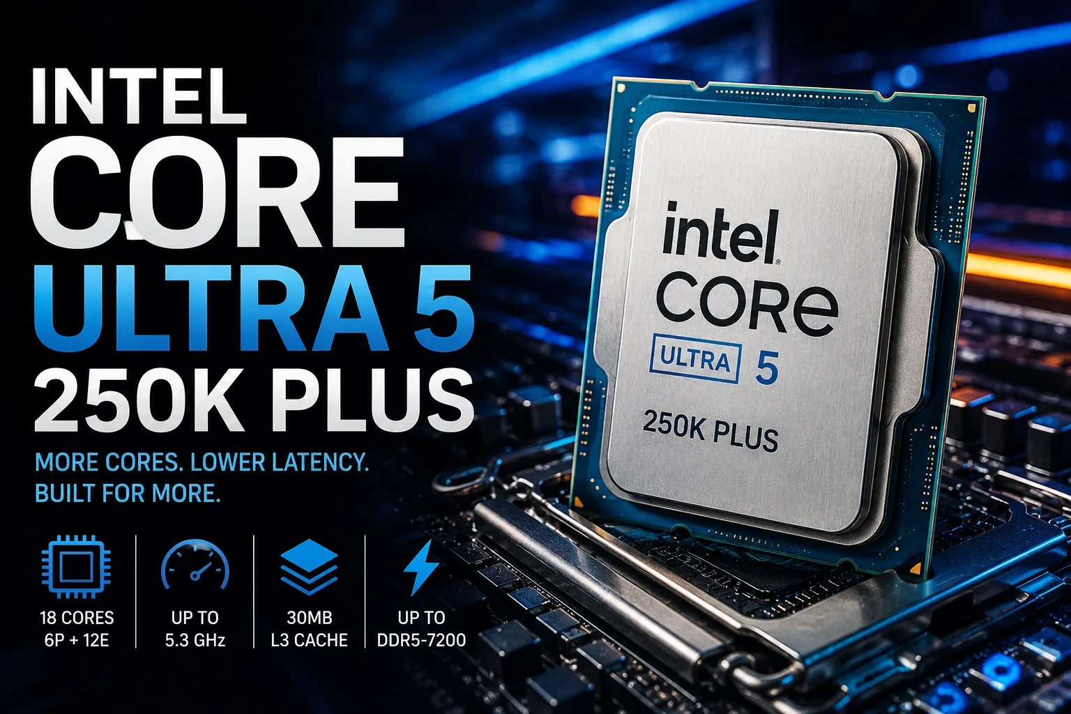
Intel Core Ultra 5 250K Plus

Intel Core Ultra 5 250K Plus: What the Core Ultra 5 Should Have Been From the Start
The Intel Core Ultra 5 250K Plus is not a cosmetic update of the 245K. Four additional E-cores have accelerated workloads, and the increased cache and faster inter-tile interface have significantly improved gaming performance. This is the Core Ultra 5 that the original Arrow Lake lineup was missing.
What Changed Compared to Core Ultra 5 245K
The Core Ultra 5 245K had six performance P-cores and eight efficient E-cores. The Core Ultra 5 250K Plus increased the number of E-cores to twelve, raising the total configuration from 14 to 18 cores.
The Arrow Lake architecture does not use Hyper-Threading, so the number of threads matches the number of physical cores.
| Feature | Core Ultra 5 250K Plus | Core Ultra 5 245K |
|---|---|---|
| P-cores | 6 | 6 |
| E-cores | 12 | 8 |
| Cores / Threads | 18 / 18 | 14 / 14 |
| Max P-core Frequency | 5.3 GHz | 5.2 GHz |
| L3 Cache | 30 MB | 24 MB |
| L2 Cache | 30 MB | 26 MB |
| Memory Support | DDR5-7200 | DDR5-6400 |
| Max Turbo Power | 159 W | 159 W |
The frequency has only increased by 100 MHz, so the primary gains come from other changes. The additional E-cores boost performance in multi-threaded applications, and the extra 6 MB of L3 cache, along with the faster inter-tile interface, help in gaming and other latency-sensitive workloads.
The number of E-cores and the amount of cache bring the model closer to the Core Ultra 7 265K. The higher-end processor still holds an advantage in P-cores: eight versus six.
Why 250K Plus Is More Practical Than the KF Version
In terms of processor specifications, the Core Ultra 5 250K Plus and 250KF Plus are identical. Both models have a configuration of 6P + 12E, a frequency up to 5.3 GHz, and 30 MB of L3 cache.
The difference lies in the integrated graphics. The K version has it, while the KF variant has it disabled. For modern gaming, the integrated core is too weak and does not replace a discrete graphics card, but it remains useful in several scenarios:
- The computer can boot without a discrete graphics card;
- It is easier to diagnose issues;
- Intel Quick Sync accelerates video processing in compatible programs.
With a small price difference, the regular 250K Plus looks more appealing. The KF model makes sense only with a noticeable discount or in a system where integrated graphics will definitely not be needed.
Gaming Performance Was Improved Not by Frequencies
The first Core Ultra 5 245K often fell behind the Ryzen 5 9600X and some older Intel processors. The issue was not only in the computational power but also in the latency when exchanging data between Arrow Lake tiles.
The Core Ultra 5 250K Plus is approximately 12% faster than its predecessor on average across gaming tests. It competes closely with the Ryzen 5 9600X: in some titles, Intel leads, while in others, AMD does.
The increase is particularly noticeable in games sensitive to memory latency and single-core speed. The additional E-cores are secondary here - the greater contribution comes from the increased cache and the faster inter-tile interface.
The Core Ultra 5 250K Plus can no longer be considered a weak gaming processor. However, Ryzen X3D models still outperform it where maximum frame rates remain the top priority.
In Workloads, Additional Cores Provide the Main Boost
The main advantage of the Core Ultra 5 250K Plus becomes apparent in programs capable of utilizing all 18 cores.
Compared to the Core Ultra 5 245K, the increase in multi-threaded tasks can reach 25-45%. In rendering, archiving, and compiling, the processor significantly outpaces typical six-core models and at times approaches the Core Ultra 7 265K.
The additional E-cores excel in the following scenarios:
- Rendering;
- Compiling large projects;
- Encoding and exporting video;
- Archiving;
- Software streaming;
- Heavy multitasking.
The advantage varies depending on the specific application. If a program does not effectively distribute the load between P-cores and E-cores, the gap narrows or disappears. Therefore, the 250K Plus shines particularly in well-parallelizable tasks rather than uniformly across all workloads.
Power Consumption and Cooling
The base power consumption of the processor is 125 W, while the maximum turbo power is 159 W. Despite the increase in core count, the power limit remains the same as that of the Core Ultra 5 245K.
In gaming, power consumption stays moderate, but during prolonged loads on all cores, the processor requires a high-performance tower cooler. An expensive liquid cooling system is not necessary, but compact entry-level models may operate noisily or limit sustained turbo performance.
The multiplier is unlocked, but significant benefits from manual overclocking are not to be expected. The rise in power consumption and heat could be more noticeable than the performance gains.
Memory and LGA1851 Platform
The Core Ultra 5 250K Plus is installed in the LGA1851 socket and works with motherboards based on Intel's 800 series chipsets. A BIOS update may be required for already released boards.
Only DDR5 is supported. The official limit has increased to DDR5-7200, but expensive DDR5-8000 is not necessary. Fast DDR5-6000 with low latencies allows for nearly full CPU performance without significant extra costs.
The future upgrade path for LGA1851 currently seems less clear than for AM5. Therefore, the 250K Plus should be chosen for its current performance rather than as a foundation for a long chain of future upgrades.
Should You Buy the Intel Core Ultra 5 250K Plus?
The Intel Core Ultra 5 250K Plus addresses the main shortcomings of the Core Ultra 5 245K. It has gained four additional E-cores, increased cache, and faster data exchange between tiles.
In gaming, the processor is about on par with the Ryzen 5 9600X, while in rendering, archiving, compiling, and encoding, it significantly outperforms typical six-core models. The K version, while retaining integrated graphics and Quick Sync, usually appears more practical than the 250KF Plus.
The processor is best suited for a versatile computer where gaming is combined with editing, programming, rendering, or other heavy workloads. For a purely gaming PC, Ryzen X3D models remain faster, but in the balance of gaming and multi-threaded performance, the Core Ultra 5 250K Plus proves to be significantly more compelling than the original Arrow Lake.
Basic
CPU Specifications
Memory Specifications
GPU Specifications
Interfaces and Ports
Benchmarks
Compared to Other CPU
Related CPU Comparisons


Share in social media
Or Link To Us
<a href="https://cputronic.com/cpu/intel-core-ultra-5-250k-plus" target="_blank">Intel Core Ultra 5 250K Plus</a>