AMD Ryzen 7 8745HS
AMD Ryzen 7 8745HS: Almost Ryzen 7 8845HS, but without Ryzen AI
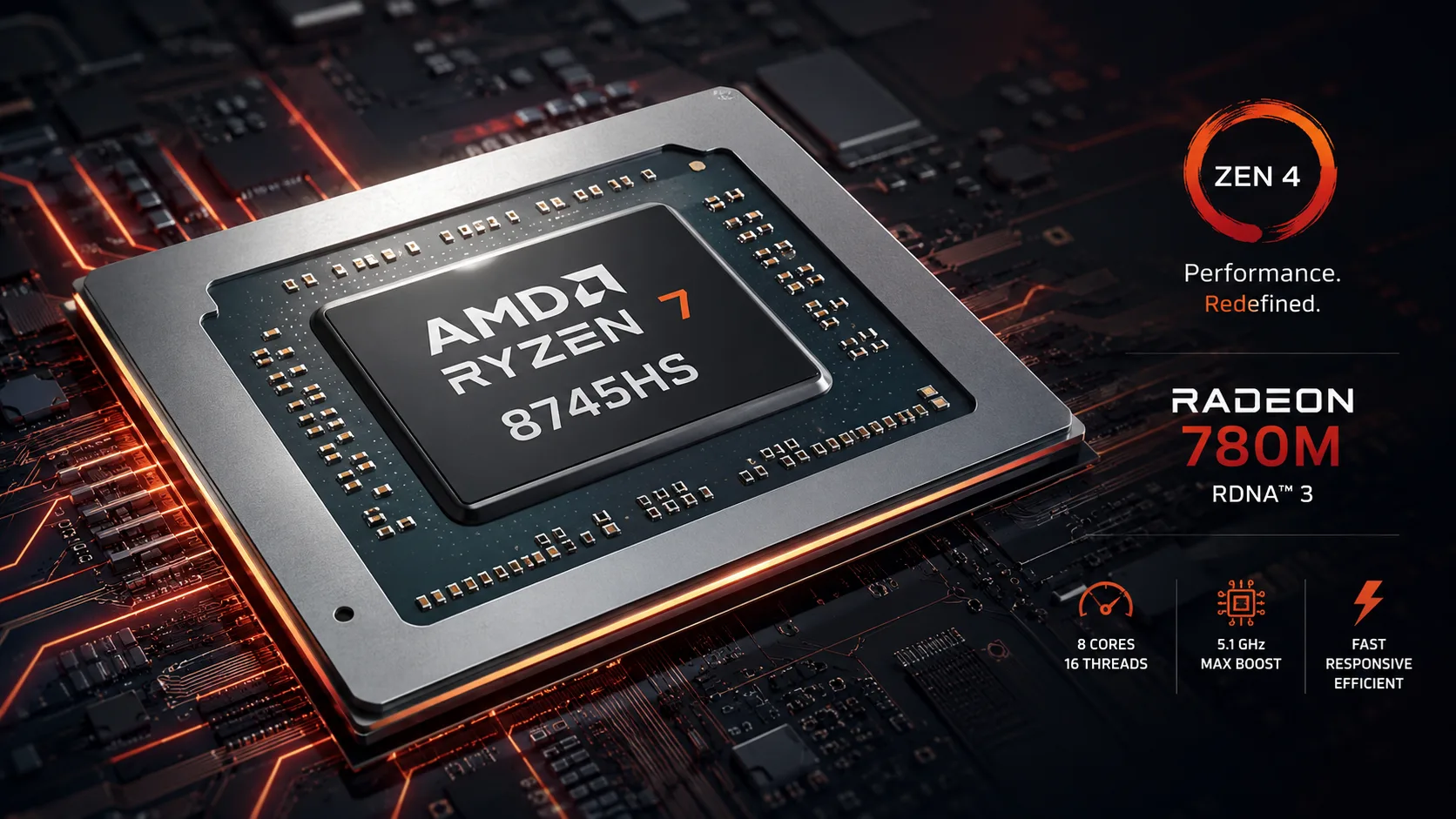
The AMD Ryzen 7 8745HS is not a new architecture and does not represent a separate step forward for mobile Ryzen processors. Its purpose is simpler: it is a fast 8-core Zen 4 processor for laptops and mini-PCs, close to the Ryzen 7 8845HS, but without the Ryzen AI block and with slightly lower clock speeds.
In terms of specifications, the processor looks solid: 8 cores, 16 threads, a clock speed of up to 4.9 GHz, 16 MB of L3 cache, a TDP of 45 W, and a configurable range of 35-54 W. The integrated graphics is the Radeon 780M with 12 RDNA 3 cores and a clock speed of up to 2600 MHz. The main loss compared to its higher counterparts is the absence of the Ryzen AI NPU.
How the Ryzen 7 8745HS Differs from the Ryzen 7 8845HS
The Ryzen 7 8745HS can be viewed as a more practical version of the Ryzen 7 8845HS for devices where the manufacturer is focusing not on AI marketing, but on price, CPU performance, and integrated graphics.
| Model | CPU | Graphics | Ryzen AI | What it means |
|---|---|---|---|---|
| Ryzen 7 8745HS | 8/16, up to 4.9 GHz | Radeon 780M, up to 2600 MHz | No | Almost the same class CPU/GPU, but without NPU |
| Ryzen 7 8845HS | 8/16, up to 5.1 GHz | Radeon 780M, up to 2700 MHz | Yes | Slightly higher clock speeds and an AI block |
| Ryzen 7 7840HS | 8/16, up to 5.1 GHz | Radeon 780M, up to 2700 MHz | Yes | Close predecessor, often more important is the price of the device |
For regular tasks, the absence of an NPU doesn't change much. Browsing, office work, development, photo processing, archiving, light editing, and mini-PCs primarily depend on the CPU, memory, SSD, and cooling. However, if the purchase is specifically made for AI functions, it seems odd to choose the 8745HS: it completely lacks Ryzen AI.
At the same time, the Ryzen 7 8845HS or Ryzen 9 8945HS should not be purchased solely for the AI block. They do have an NPU, but its usefulness depends on specific applications. Therefore, the main question becomes simpler: do you specifically need an NPU, or is it sufficient to have a powerful CPU and Radeon 780M?
Performance
In terms of CPU, the Ryzen 7 8745HS is on par with good 8-core HS-class Zen 4 processors. It does not reach the HX-class for heavy workstations, but it offers a very respectable performance for a compact laptop or mini-PC.
| Test | AMD Ryzen 7 8745HS |
|---|---|
| Geekbench 6 Single-Core | ≈ 2395 |
| Geekbench 6 Multi-Core | ≈ 10921 |
| Cinebench R23 Single-Core | ≈ 1602 |
| Cinebench R23 Multi-Core | ≈ 14565 |
In single-threaded tasks, the processor is fast enough for a responsive system, heavy browsing, and most work applications. In multi-threaded tasks, 8 cores and 16 threads allow for smooth operation with IDEs, virtual machines, batch image processing, and moderate editing.
However, the results depend heavily on the device. In a mini-PC with good cooling, the 8745HS can maintain high multi-threaded performance, while in a cramped case, it may quickly hit power and temperature limits. Thus, the difference between two systems with the same processor can be more significant than it appears based on the CPU name.
Radeon 780M: Strong iGPU, but Memory Matters
The Radeon 780M is one of the main reasons to consider the Ryzen 7 8745HS. This is an RDNA 3 integrated graphics solution with 12 compute units, 768 shaders, and a clock speed of up to 2600 MHz in this processor version. It does not have dedicated video memory: the iGPU uses system RAM, so dual-channel DDR5 or fast LPDDR5X is critical for performance.
In synthetic benchmarks, the Radeon 780M is noticeably faster than older Vega iGPUs, but it is still far from a normal discrete graphics card. For the Ryzen 7 8745HS, it's best to aim for performance ranges adjusted for the 2600 MHz frequency, memory, and power limits of the specific device.
| Test | Estimated Result |
|---|---|
| 3DMark Time Spy Graphics | ≈ 2400-2700 |
| 3DMark Fire Strike Graphics | ≈ 6900-7500 |
| 3DMark Night Raid Graphics | ≈ 30000-34000 |
| Unigine Superposition 1080p Medium | ≈ 4100-4800 |
In games, the Radeon 780M is best viewed as a solution for 1080p on low or medium settings. FPS numbers are indicative for systems with fast dual-channel memory; results may be lower in weaker configurations.
| Game | Settings | Estimated FPS |
|---|---|---|
| Dota 2 | 1080p, high/Best Looking | ≈ 70-80 FPS |
| Far Cry 5 | 1080p, Low | ≈ 50 FPS |
| Far Cry 6 | 1080p, Low | ≈ 40-45 FPS |
| Shadow of the Tomb Raider | 1080p, Low | ≈ 58-65 FPS |
| Shadow of the Tomb Raider | 1080p, Medium | ≈ 35-37 FPS |
| The Witcher 3 | 1080p, Low/Medium | ≈ 45-50 FPS |
The main takeaway: the Radeon 780M shines as integrated graphics. It is suitable for video playback, multiple monitors, older games, esports titles, and light gaming without a discrete graphics card. For serious gaming, however, memory, cooling, and real-world benchmarks of specific models remain important.
Availability Nuance
AMD indicates a regional availability of "China" for the Ryzen 7 8745HS. Because of this, the model seems a bit unusual; it is not as widely found in classic laptops as the Ryzen 7 8845HS or Ryzen 7 7840HS.
However, the processor can be seen in mini-PCs and OEM systems that are sold across multiple regions. Therefore, when purchasing, it's more important to look not at the mere existence of the 8745HS but at the specific device: cooling, memory, power limits, ports, and price.
Is it Worth Buying the AMD Ryzen 7 8745HS?
It's worth considering the AMD Ryzen 7 8745HS not for its AI capabilities, but for its strong 8-core CPU, Radeon 780M, and the favorable price of the specific device. It is a good option for mini-PCs and high-performance laptops, provided you don't need the Ryzen AI NPU.
The key point is not to consider it a complete copy of the Ryzen 7 8845HS. The 8745HS has slightly lower CPU and iGPU clock speeds and lacks the AI block entirely. However, for regular work, development, media use, mini-PCs, and light gaming, this is not a critical loss. If the device is well-cooled and has adequate memory, the Ryzen 7 8745HS appears to be a very reasonable choice.
Basic
CPU Specifications
Memory Specifications
GPU Specifications
Interfaces and Ports
Benchmarks
Compared to Other CPU
Related CPU Comparisons


Share in social media
Or Link To Us
<a href="https://cputronic.com/cpu/amd-ryzen-7-8745hs" target="_blank">AMD Ryzen 7 8745HS</a>