NVIDIA Tesla P40
NVIDIA Tesla P40: Why Run LLMs on a 2016 Graphics Card?
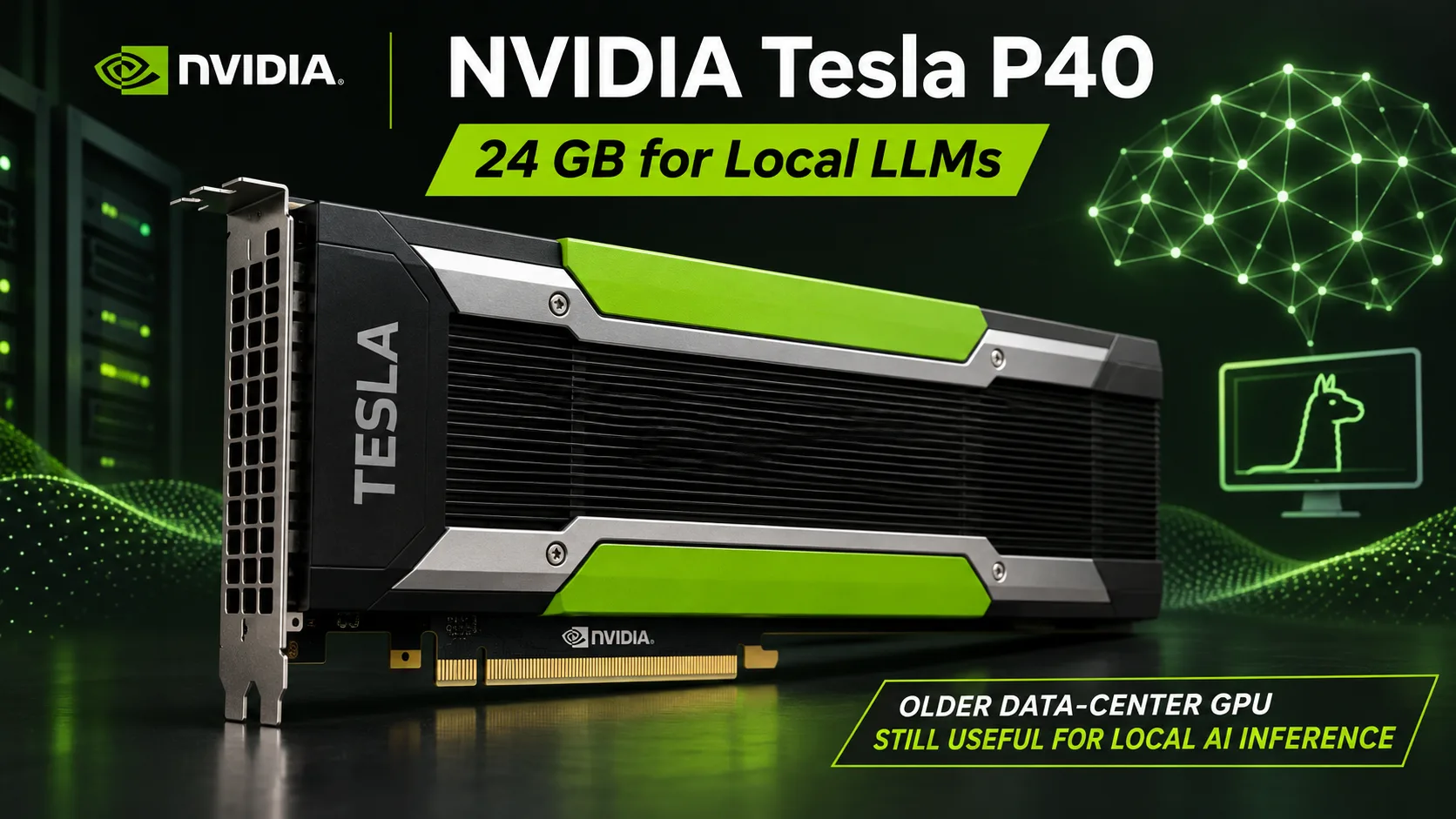
The NVIDIA Tesla P40 was introduced in 2016 as a server accelerator for neural networks. Ten years later, it is attracting attention because of its 24 GB of video memory. That is enough to run some language models with 30-32 billion parameters, which do not fit into the video memory of most inexpensive gaming GPUs.
However, the Pascal architecture places significant limits on performance. The Tesla P40 has no Tensor Cores, FP16 computations are slow, and its passive cooling requires modification when the card is installed in a regular computer. How useful is its 24 GB in 2026?
24 GB of Memory on the Pascal Architecture
The Tesla P40 is built around the GP102 chip, related to the GeForce GTX 1080 Ti. It has 3840 CUDA cores, and the GPU clock speed ranges from 1303 to 1531 MHz. The card is equipped with GDDR5 memory on a 384-bit bus, with a bandwidth of 346 GB/s.
Unlike the Tesla P100, which uses the GP100 chip and HBM2 memory, the P40 was primarily designed for neural network inference. Its FP16 performance is approximately 0.19 TFLOPS-about 64 times lower than its FP32 performance.
| Graphics card | Memory | Memory bandwidth | FP16 | Tensor Cores |
|---|---|---|---|---|
| NVIDIA Tesla P40 | 24 GB GDDR5 | 346 GB/s | ~0.19 TFLOPS | No |
| NVIDIA Tesla P100 PCIe | 16 GB HBM2 | 732 GB/s | 18.7 TFLOPS | No |
| NVIDIA Tesla V100 PCIe | 32 GB HBM2 | 900 GB/s | ~28 TFLOPS | 640 |
NVIDIA specified up to 12 TFLOPS in FP32 and 47 TOPS in INT8 for the P40. However, these figures cannot be directly translated into the speed of modern LLMs. The result depends on the model format, the computational operations used, and software optimization.
Performance in llama.cpp Tests
Text-generation tests are the most representative for the Tesla P40. The results below were obtained in llama.cpp using the Llama 2 7B model with Q4_0 quantization.
| Graphics card | Memory | Prompt processing, tok/s | Generation, tok/s |
|---|---|---|---|
| NVIDIA Tesla P40 | 24 GB | 1007 | 54.7 |
| NVIDIA Tesla P100 | 16 GB | 761 | 58.4 |
| NVIDIA Tesla V100 | 32 GB | 3043 | 129.1 |
| NVIDIA GeForce RTX 3060 | 12 GB | 2138 | 75.6 |
| NVIDIA GeForce RTX 3090 | 24 GB | 5175 | 158.2 |
llama-bench test: processing 512 input tokens (pp512) and generating 128 tokens (tg128), using CUDA without Flash Attention. The results were obtained on different systems and llama.cpp versions, so the comparison is approximate.
When generating text, the Tesla P40 falls only slightly behind the P100, despite having substantially lower memory bandwidth. The RTX 3060 is approximately 38% faster, while the RTX 3090 is nearly three times as fast.
The difference is greater when processing the input prompt: the RTX 3090 is more than five times faster than the P40. This is particularly noticeable when working with long documents, when thousands of input tokens must be processed before a response can be generated.
However, Llama 2 7B fits even into 8 GB of video memory. This test demonstrates GPU speed but does not reveal the P40’s main advantage-the ability to run larger models.
Which LLMs Fit into 24 GB
A good example is Qwen2.5-32B-Instruct. In the GGUF format with Q4_K_M quantization, the model weights occupy approximately 19.9 GB. The Tesla P40 has enough space left for the KV cache and computational buffers, although the available context length depends on the launch settings.
This model will not fit entirely on an RTX 3060 with 12 GB. More aggressive quantization will be required, or part of the computation will have to be offloaded to system memory.
The Tesla P40’s capabilities depend on the model’s size and format:
- 7B-8B: Enough memory for Q4, Q8, and a relatively long context.
- 14B: Many models fit even in Q8_0, leaving memory for auxiliary data.
- 30B-32B: Q4 is possible with an appropriate KV-cache size and sufficient space for other buffers.
Capacity should not be confused with performance. A model with 32 billion parameters requires significantly more computation than Llama 2 7B. The results above cannot be used to estimate its speed without separate testing.
For local execution of quantized GGUF models, llama.cpp can be used with a compatible CUDA backend. The P40’s limitations become more noticeable when processing large documents frequently or serving multiple users simultaneously.
Installing It in a Regular Computer
The Tesla P40 is designed for servers with forced-air cooling. The card has no built-in fan, and its maximum power consumption reaches 250 W.
The following factors must be taken into account during installation:
- Cooling. Directed airflow through the heatsink is required, usually provided by a separate fan and duct.
- Power. The card uses a server CPU/EPS 8-pin connector. A standard PCIe 8-pin cable must not be connected directly in its place.
- Video outputs. HDMI and DisplayPort are absent. A monitor will have to be connected to another graphics adapter.
- Dimensions. The board is approximately 267 mm long and occupies two slots.
Another limitation concerns software support. The Tesla P40 has Compute Capability 6.1. With CUDA Toolkit 13.0, NVIDIA discontinued support for compiling applications for Pascal.
Building software for this architecture requires CUDA Toolkit 12.9 or an earlier compatible version. The latest NVIDIA driver branch supporting Pascal is R580, whose maintenance is scheduled to continue until June 2028.
This does not mean that the P40 will stop working after that date. However, newer versions of computational libraries may require more modern GPUs, so software compatibility must be checked separately.
Is the Tesla P40 Worth Using in 2026?
The Tesla P40 retains practical value because of its 24 GB of memory. It can run quantized LLMs that do not fit on an RTX 3060 with 12 GB or a Tesla P100 with 16 GB. At the same time, both of those cards may be faster in tasks that do not require a large amount of video memory.
The RTX 3090, with the same 24 GB, significantly outperforms the P40 in both generation speed and prompt processing. The Tesla V100 is also substantially faster, but the 16 GB version limits the choice of large models, while the 32 GB version solves this problem.
When choosing a P40, the cost of the card itself is not the only factor to consider. Additional cooling, suitable power delivery, power consumption of up to 250 W, and the need to use a compatible software stack all increase operating costs.
The Tesla P40 makes sense if local LLMs specifically require 24 GB of memory, high speed is not essential, and the cost of a complete system is significantly lower than the alternatives. For a new workstation intended for long-term use, a more modern GPU is preferable.
GPU Comparison
Compare Tesla P40 with other GPUs
Basic
Memory Specifications
Display and Media
Theoretical Performance
Miscellaneous
Benchmarks
Compared to Other GPU
Related GPU Comparisons


Share in social media
Or Link To Us
<a href="https://cputronic.com/gpu/nvidia-tesla-p40" target="_blank">NVIDIA Tesla P40</a>