NVIDIA GB10
NVIDIA GB10: 1 PFLOP and 128 GB Memory for Local AI
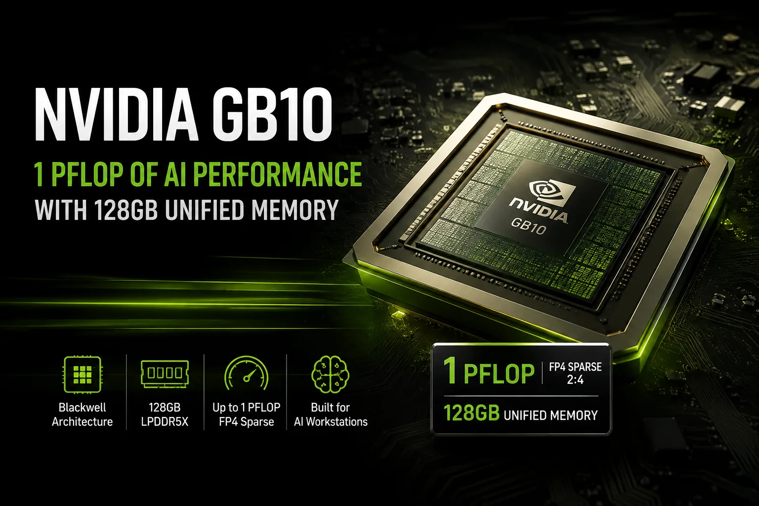
The GB10 is designed for compact AI stations like the NVIDIA DGX Spark and significantly differs from typical Blackwell graphics cards. It combines a 20-core Arm processor, Blackwell graphics, and 128 GB of LPDDR5X unified memory in a single enclosure. NVIDIA claims performance of up to 1 PFLOP FP4, and real-world tests confirm this level. In practical AI tasks, memory bandwidth becomes a crucial limitation.
How GB10 Differs from GeForce
The GB10 was first showcased in January 2025 as part of Project DIGITS. Later, this concept formed the basis for the DGX Spark, with the platform being adopted by other manufacturers. Systems based on the GB10 include the ASUS Ascent GX10, Lenovo ThinkStation PGX, HP ZGX Nano G1n, GIGABYTE AI TOP ATOM, Acer Veriton GN100, and other compact AI systems.
The main advantage of the GB10 lies in its 128 GB of unified memory for both CPU and GPU.
Due to this memory capacity, the GB10 can locally run models that cannot fit into the 16-32 GB VRAM of most consumer graphics cards. According to NVIDIA, systems on the GB10 can handle models with up to 200 billion parameters with appropriate quantization and optimizations.
Tests Confirm the Claimed 1 PFLOP
The 1 PFLOP figure pertains to FP4 computations with a sparsity of 2:4. This number cannot directly correlate with the overall speed of the graphics section or the speed of token generation in LLM.
In 2026, reproducible results from nvfp4bench appeared, which test the Tensor Cores of the GB10 in NVFP4 calculations. Production systems show approximately 486-504 TFLOPS in dense NVFP4 and about 1 PFLOP with a sparsity of 2:4.
GB10 in Specific Devices
| Device | NVFP4 Dense | NVFP4 Sparse 2:4 | Memory Bandwidth |
|---|---|---|---|
| HP ZGX Nano G1n | 503.9 TFLOPS | 1007.8 TFLOPS | 207 GB/s |
| Lenovo ThinkStation PGX | 498.4 TFLOPS | 996.7 TFLOPS | 213 GB/s |
| ASUS Ascent GX10 | 497.5 TFLOPS | 994.8 TFLOPS | 205 GB/s |
| GIGABYTE AI TOP ATOM | 496.6 TFLOPS | 993.4 TFLOPS | 214 GB/s |
| NVIDIA DGX Spark | 486.3 TFLOPS | 973.2 TFLOPS | 207 GB/s |
All results were obtained using the same test type, allowing for direct comparisons. The variation among systems is minor, and differences in enclosure, cooling, and configuration have little effect on the final result.
Memory Bandwidth Limitation
Tensor Cores deliver high performance at low precision, while the official bandwidth of the 128 GB LPDDR5X reaches up to 273 GB/s. In practical tests, systems typically demonstrate around 200-214 GB/s.
For local inference of LLM, this metric is particularly important. During sequential token generation, model weights are constantly read from memory, so speed is often limited by memory bandwidth.
Therefore, 1 PFLOP cannot be directly translated into the operational speed of a specific neural network.
With long pre-fills, batch processing, and parallel requests, Tensor Cores load more efficiently. The GB10 can accommodate models in its unified memory that cannot fit into the VRAM of a single consumer graphics card.
The amount of memory is large, but its bandwidth is notably lower than that of GDDR7 on powerful discrete GPUs.
How Many Tokens Per Second Does GB10 Output?
Practical LLM tests reveal the character of the GB10 more effectively than the peak FP4 performance. On the NVIDIA DGX Spark with Ollama 0.18.3 and CUDA 13.0, the speed noticeably declines as the dense model grows, but the 128 GB of memory allows for the running of models that do not fit on most consumer graphics cards.
| Model | Memory Size | Generation Rate | Request Processing |
|---|---|---|---|
| Llama 3.1 8B | 4.9 GB | 42.86 tok/s | 574.79 tok/s |
| Qwen3 32B | 20 GB | 9.88 tok/s | 141.91 tok/s |
| Llama 3.1 70B | 42 GB | 4.76 tok/s | 67.92 tok/s |
| Mistral Large 123B | 73 GB | 2.28 tok/s | 10.43 tok/s |
The results clearly demonstrate the limitation of LPDDR5X. Llama 3.1 8B generates about 43 tokens per second, while Llama 3.1 70B reduces the rate to around 4.8 tokens per second. Mistral Large 123B operates even slower, but the very ability to fit such a large model in the memory of a compact system is one of the advantages of the GB10.
The model architecture also significantly affects the outcome. In individual tests, llama.cpp Qwen3 30B with the MoE architecture showed around 89 tokens per second, while the dense Qwen3 32B achieved about 11 tokens per second. In MoE, only a portion of the parameters are used during generation, thus making such a model considerably less dependent on the GB10's memory bandwidth.
How Much Do Computers with GB10 Cost?
By August 2026, the GB10 is utilized in several production systems. The chip's performance varies slightly, while the prices and storage capacity depend significantly on the specific model.
| System | Storage | Starting Price |
|---|---|---|
| ASUS Ascent GX10 | 1 TB | approximately €3,999 |
| Lenovo ThinkStation PGX | 1 TB | approximately €4,733 |
| HP ZGX Nano G1n | 2 TB | approximately €5,199 |
| GIGABYTE AI TOP ATOM | 4 TB | approximately €5,499 |
| NVIDIA DGX Spark Founders Edition | 4 TB | approximately €5,599 |
| Acer Veriton GN100 | 4 TB | approximately €5,999 |
Prices reflect offers in the European market and depend on the specific configuration.
In terms of price-performance ratio, the ASUS Ascent GX10 appears to be more favorable than the rest. It is over €1,000 cheaper than some competitors, and NVFP4 results differ by only a few percent.
The higher costs of more expensive models often come from the SSD, port selection, warranty, and support. They do not provide a significant performance boost for the GB10.
How Project DIGITS, DGX Spark, and GB10 Are Related
The GB10 has several related names that emerged at different stages of the platform's development. In January 2025, NVIDIA introduced a platform called Project DIGITS. Later, NVIDIA's proprietary system was named DGX Spark, and the GB10 began to be used by ASUS, Lenovo, HP, GIGABYTE, and other manufacturers.
| Title | Description |
|---|---|
| Project DIGITS | initial concept of a compact AI computer |
| NVIDIA GB10 | Grace Blackwell Superchip |
| NVIDIA DGX Spark | proprietary production system from NVIDIA on GB10 |
| ASUS GX10, Lenovo PGX, HP ZGX, and others | OEM systems on the same platform |
The ASUS GX10, Lenovo PGX, and HP ZGX utilize the same GB10 computing platform. Differences among these systems primarily concern the case, storage, cooling, and peripherals.
The GB10 is better viewed as a specialized SoC for AI workstations. The graphics portion uses the Blackwell architecture, and the platform integrates CPU, GPU, and unified memory in one solution.
Conclusion
With a starting price of around €4,000, the GB10 is aimed at a narrow range of tasks. If the required model fits into the VRAM of a standard RTX, a discrete graphics card is often more likely to provide greater computational performance for the same money.
The advantage of the GB10 emerges in tasks where 24-32 GB of VRAM is no longer sufficient. Its 128 GB of unified memory allows for the local deployment of large AI models without multiple discrete GPUs and the complexity of distributing weights among them.
Real systems confirm the claimed level of around 1 PFLOP FP4 at a sparsity of 2:4. Practical LLM tests also show the limitation of LPDDR5X bandwidth: large dense models fit into memory but generate tokens relatively slowly. The strength of the GB10 lies in the combination of 128 GB of unified memory, CUDA, and a compact form factor.
GPU Comparison
Compare GB10 with other GPUs
Basic
Memory Specifications
Display and Media
Theoretical Performance
Miscellaneous
Benchmarks
Compared to Other GPU
Related GPU Comparisons

Share in social media
Or Link To Us
<a href="https://cputronic.com/gpu/nvidia-gb10" target="_blank">NVIDIA GB10</a>