NVIDIA GeForce RTX 5090 D V2
NVIDIA GeForce RTX 5090 D V2: 24 GB Instead of 32, But Gaming Performance Remains Largely Untouched
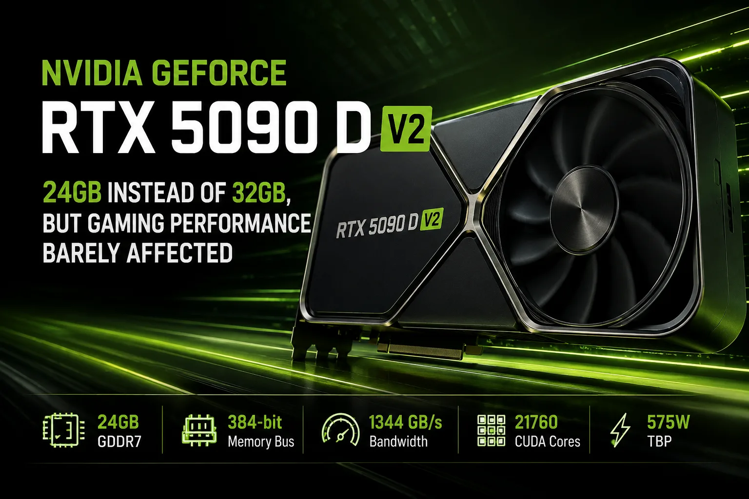
The GeForce RTX 5090 D V2 emerged after another round of tightening U.S. export restrictions, replacing the original RTX 5090 D in the Chinese market. NVIDIA reduced the memory from 32 GB to 24 GB, the bus width from 512 to 384 bits, and the bandwidth from 1792 to 1344 GB/s. However, the GPU itself was hardly scaled down, so in most gaming benchmarks, the performance difference turned out to be minor.
What Changed in V2
The RTX 5090 D V2 retained 21,760 CUDA cores, 680 Tensor Cores, 170 RT Cores, a Boost clock of around 2.41 GHz, and a 575-watt power limit. The claimed AI performance also remains the same at 2375 AI TOPS.
The main changes affected the memory. Instead of 32 GB and a 512-bit bus, the V2 received 24 GB of GDDR7 with a 384-bit interface. With a memory speed of 28 Gbps, the bandwidth decreased to 1344 GB/s, exactly one-quarter lower.
For most modern games, 24 GB is still ample for high settings. However, V2 replaces the 32 GB version while retaining nearly the same GPU and power consumption.
How Much V2 Lost in Gaming Performance
In Time Spy, the reduction in bus width by a quarter hardly impacted the score.
On the GALAX GeForce RTX 5090 D V2 HOF, the result in 3DMark Time Spy Extreme was 25,479 points, whereas the original RTX 5090 D scored 25,690. In standard Time Spy, the new card recorded 49,285, compared to 48,922 points for the initial version.
| Graphics Card | 3DMark Time Spy | Time Spy Extreme |
|---|---|---|
| GALAX RTX 5090 D V2 HOF | 49,285 | 25,479 |
| RTX 5090 D | 48,922 | 25,690 |
The difference is about one percent. Gaming tests yield similar results: in Black Myth: Wukong and Monster Hunter: Wilds, the metrics of the two versions are almost identical, while in Cyberpunk 2077 and Red Dead Redemption 2, the gap remains small.
Even after the cut, the bandwidth remains very high at 1344 GB/s. In 4K, a narrower bus rarely becomes the primary limitation of the card.
Specific RTX 5090 D V2 Models
NVIDIA's partners have released V2 versions with various cooling systems, clock speeds, and power limits.
| Model | Features |
|---|---|
| INNO3D GeForce RTX 5090 D V2 X3 | Three-fan model with published gaming tests at 4K |
| Colorful iGame RTX 5090 D V2 Vulcan OC | Vapor chamber and increased power limit |
| ASUS ROG Astral RTX 5090 D V2 | Higher factory Boost clock and increased power requirements |
The INNO3D GeForce RTX 5090 D V2 X3 hit around 210 FPS in Cyberpunk 2077 at 4K, RT Overdrive, DLSS Quality, and Multi Frame Generation 4x. In Black Myth: Wukong at 4K, maximum quality, full RT, and the same DLSS settings, it achieved about 184 FPS.
These values cannot be directly compared to tests without Frame Generation. They show the performance of a specific model utilizing DLSS 4 rather than the raw GPU performance.
The Colorful iGame RTX 5090 D V2 Vulcan OC features a vapor chamber and a multi-pipe cooling system. Due to the increased power limit, consumption under load can exceed the standard 575 W.
Overclocked models have even higher frequencies and power requirements. Some ASUS ROG Astral RTX 5090 D V2 versions operate significantly above the reference 2407 MHz and require a power supply of up to 1200 W.
Loss of 8 GB Affects AI More Than Gaming
In professional workloads, the V2 falls significantly behind the original RTX 5090 D.
In most modern games, 24 GB is currently sufficient even for heavy settings, but for local language models, image generation, and complex 3D scenes, VRAM capacity can be critical.
If the workload exceeds 24 GB, losing 8 GB clearly doesn’t just translate to a few percentage points: it necessitates model reduction, decreased accuracy, or offloading some data to system memory.
Thus, in gaming, the RTX 5090 D and D V2 differ little, while for local AI tasks, the 32 GB version has a noticeable advantage.
Why Power Consumption Remains the Same
Despite the reduced memory, the standard TBP remains unchanged at 575 W. The GPU frequencies and the number of compute units have not changed either.
Therefore, the system requirements are nearly unchanged: a powerful PSU, a well-ventilated case, and ample space for a large graphics card are needed. For most off-the-shelf models, manufacturers recommend a power supply of 1000 W.
Overclocked models have higher limits, so when choosing, it's essential to consider the BIOS, cooling, and real power consumption, and not just the Boost clock.
RTX 5090 D vs RTX 5090 D V2
| Feature | RTX 5090 D | RTX 5090 D V2 |
|---|---|---|
| Video Memory | 32 GB GDDR7 | 24 GB GDDR7 |
| Memory Bus | 512 bits | 384 bits |
| Bandwidth | 1792 GB/s | 1344 GB/s |
| CUDA Cores | 21,760 | 21,760 |
| Boost | 2407 MHz | 2407 MHz |
| TBP | 575 W | 575 W |
| AI Performance | 2375 AI TOPS | 2375 AI TOPS |
For AI and professional tasks, the additional 8 GB of the original RTX 5090 D may matter much more than a few percentage points of performance.
Conclusion
The RTX 5090 D V2 lost a quarter of its memory and bandwidth, but the computational part of the GPU changed very little. Therefore, in gaming, the losses are minor, while the memory reduction significantly impacts AI and professional tasks.
If both versions are priced the same, the 32 GB RTX 5090 D is preferable. If the V2 is substantially cheaper and the card is primarily needed for 4K gaming, losing 8 GB by itself does not make it a bad choice.
GPU Comparison
Compare GeForce RTX 5090 D V2 with other GPUs
Basic
Memory Specifications
Display and Media
3x DisplayPort 2.1b
Theoretical Performance
Miscellaneous
Benchmarks
Compared to Other GPU
Related GPU Comparisons

Share in social media
Or Link To Us
<a href="https://cputronic.com/index.php/gpu/nvidia-geforce-rtx-5090-d-v2" target="_blank">NVIDIA GeForce RTX 5090 D V2</a>