NVIDIA B300

NVIDIA B300: Why Blackwell Ultra Received 288 GB of HBM3E
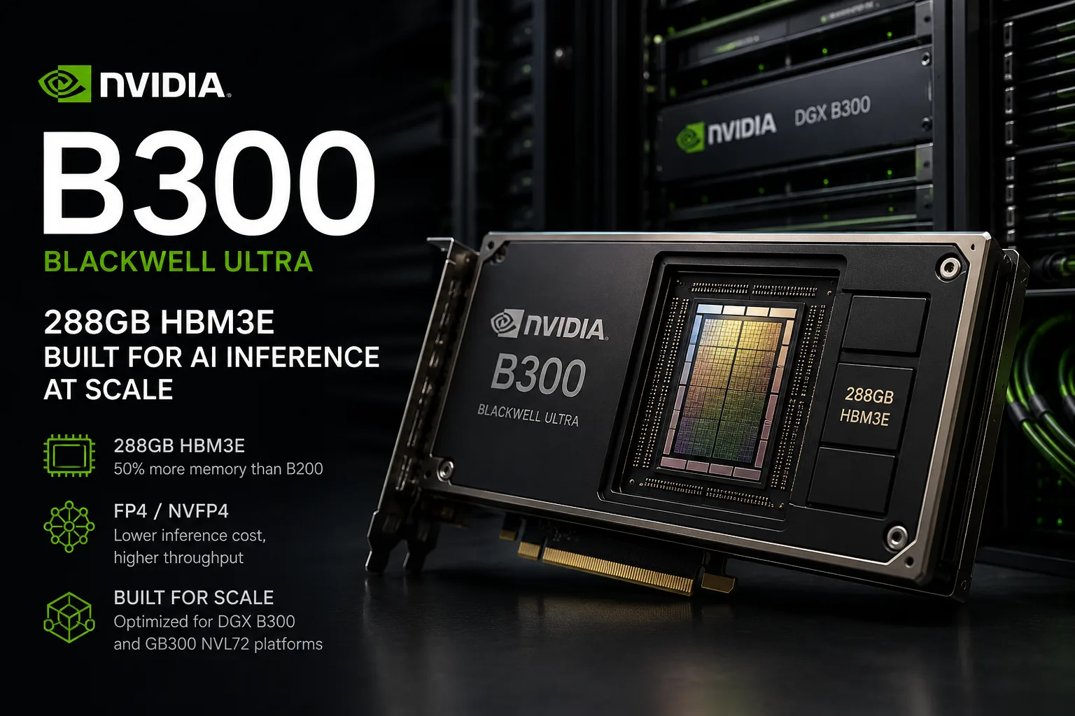
NVIDIA B300 is a data center accelerator of the Blackwell Ultra generation. The main difference from the B200 is the increased memory size: 288 GB of HBM3E instead of 192 GB. For large AI models, this increase may be more important than peak performance, as long contexts and concurrent requests quickly hit memory limits.
Large language models need to store not only weights but also intermediate data, including KV-cache. The longer the request, the more reasoning steps are required, and the higher the parallel load, the faster the HBM usage. The B300 is designed for large LLMs, MoE models, long documents, and inference with a high number of simultaneous requests.
What is NVIDIA B300
The B300 belongs to the Blackwell Ultra family-an enhanced version of Blackwell for servers and AI infrastructure. It is not a consumer graphics card nor an accelerator for standard workstations. Its place is in data centers, DGX systems, and rack-level platforms such as GB300 NVL72.
It is important to distinguish the names. B300 refers to the accelerator itself. DGX B300 is an NVIDIA server with eight of these GPUs. GB300 NVL72 is a rack-level system where dozens of Blackwell Ultra GPUs are combined with fast NVLink interconnect.
The B300 is best considered not as a standalone board, but as part of a platform. NVIDIA sells not only GPUs but also a bundle of NVLink, NVSwitch, networking solutions, CUDA, TensorRT-LLM, and ready-made server configurations.
The Main Upgrade - 288 GB HBM3E
The B300 has up to 288 GB of HBM3E per GPU. This is a key characteristic for the inference of large language models. The B200 has a lower memory capacity-up to 192 GB-so the increase with the B300 is not just formal but significant for real workloads: more space for the model, longer context, and parallel requests.
Especially important is the KV-cache. These are the data the model stores during generation to avoid recalculating the entire previous context from scratch. The longer the dialogue, document, or chain of reasoning, the more memory this cache occupies. If many users are served simultaneously, the load on the HBM increases even more rapidly.
The additional 96 GB of memory compared to the B200 can provide more benefits than an increase in computational units. They allow more data to be kept in the GPU's memory, reduce the need to shard the model across accelerators, and decrease data transfer time. For a data center, this affects response latency, the number of concurrent requests, and generation costs.
Why B300 is Important for Long Contexts and Reasoning
AI inference is becoming more demanding. Previously, a typical request to a model was often short: a question and an answer. Now, models work with large documents, codebases, tools, and tasks that require several reasoning steps. Such scenarios create more intermediate data and put more strain on memory.
Therefore, the B300 appears not merely as an upgraded version of the B200 but as the next step in Blackwell for mass inference. The H200 was a powerful accelerator of the Hopper generation. The B200 was the first significant transition to Blackwell. The B300 enhances this line with a larger HBM capacity and a better focus on long contexts.
For such tasks, comparing only TFLOPS provides little insight. What matters more is how many users can be served by a single GPU, how long a context the system can handle, and the cost of producing a response.
FP4 and NVFP4: Performance for Inference
For the B300, traditional FP32 metrics are secondary. The main area of focus for this accelerator is Tensor Cores and low-precision computations: FP8, FP4, and the proprietary NVFP4 format. It is in this area that NVIDIA seeks to reduce inference costs.
Low precision reduces data volume and accelerates computations. If a model can be effectively run in FP4 without noticeable quality loss, the data center achieves more tokens per second with the same infrastructure. Therefore, the B300 should be evaluated not as a universal GPU, but as an accelerator for models optimized for such formats.
The hardware works in conjunction with the software stack. CUDA, TensorRT-LLM, Transformer Engine, and ready-made optimizations for LLM help achieve real performance, not just good figures in specifications.
How B300 Differs from B200 and H200
The B300 does not introduce a new architecture following the B200. It is the evolution of Blackwell with a stronger emphasis on memory and inference. The main difference from the B200 is the 288 GB of HBM3E instead of 192 GB. For long contexts, KV-cache, and parallel request servicing, such an increase can be critical.
The difference from the H200 runs deeper. The H200 belongs to the Hopper generation and was also designed for heavy AI tasks, but the B300 transitions to Blackwell Ultra: more capabilities for low precision, higher inference density, and better scaling within NVIDIA’s new server platforms.
Therefore, the B300 should be viewed not as a simple upgrade of the accelerator in a server but as part of the transition from model training to their continuous operation. Training is an expensive, but time-limited stage. Inference operates continuously and more rapidly impacts costs.
DGX B300 and GB300 NVL72
The DGX B300 illustrates how NVIDIA envisions this accelerator in practice. It is not a set of individual boards but a ready-made AI server with eight B300s, large GPU memory, fast interconnect, and networking interfaces for clusters.
The GB300 NVL72 is the next level: a rack with dozens of Blackwell Ultra GPUs and Grace CPUs. In such a system, the B300 operates as part of an overall computing platform. For large models, this is essential: the faster the GPUs exchange data, the less downtime for computational units and the more effective the utilization of expensive hardware.
In large AI workloads, what matters is not just a single specification figure but the stable scaling of the entire system. Therefore, NVIDIA promotes not only GPUs but also ready-made servers and racks.
Competitors: AMD is Close on Hardware, NVIDIA is Stronger on Platform
The main competitor to the B300 is the AMD Instinct MI355X. It is also aimed at heavy AI workloads and offers a large amount of HBM3E. By specific characteristics, AMD can no longer be considered a player significantly lagging in hardware.
However, in data centers, memory is not the only deciding factor. Large customers care about the software stack, support for popular models, scaling between GPUs, and the availability of ready-made server solutions. NVIDIA holds a strong position here due to CUDA, TensorRT-LLM, Transformer Engine, NVLink/NVSwitch, and a large number of LLM inference optimizations.
AMD may be attractive where price, openness, and reducing dependence on NVIDIA matter. But if a company needs the most predictable infrastructure for large models, the B300 appears to be a more obvious choice.
Limitations of B300
The B300 is a powerful but complex accelerator to operate. It cannot be evaluated separately from power, cooling, network, and rack costs. At this level, infrastructure directly affects the total cost of ownership.
For a small lab, the B300 may be excessive. Its advantages are revealed where there are large models, constant inference load, an optimized stack, and tasks that effectively utilize FP4, HBM, and fast inter-GPU communication.
There is also a strategic nuance: the B300 is an enhancement of Blackwell, not the latest generation of NVIDIA. The company is already preparing the next architectures, so the B300 is interesting as the top version of Blackwell Ultra for the upcoming cycle of AI infrastructure.
Conclusion
The NVIDIA B300 is important not just for a record number but for the combination of 288 GB of HBM3E, high memory bandwidth, FP4/NVFP4, and scaling through the NVIDIA platform. It is an accelerator for tasks where not just the chip price matters, but also response cost, latency, and the number of requests per rack.
The B300 is not for everyone. It is too expensive and specialized for regular computations. But for clouds, AI companies, and large data centers, it is one of the key accelerators of the Blackwell Ultra generation. It shows a market shift: an individual GPU is no longer what matters; it’s the complete system that reliably serves large models under realistic loads.
Basic
Memory Specifications
Display and Media
Theoretical Performance
Miscellaneous
Benchmarks
Compared to Other GPU
Related GPU Comparisons

Share in social media
Or Link To Us
<a href="https://cputronic.com/index.php/gpu/nvidia-b300" target="_blank">NVIDIA B300</a>