NVIDIA Tesla K80
vs
NVIDIA Tesla P40
GPU Comparison Result
NVIDIA Tesla K80 vs Tesla P40: Same 24 GB, but Different Capabilities
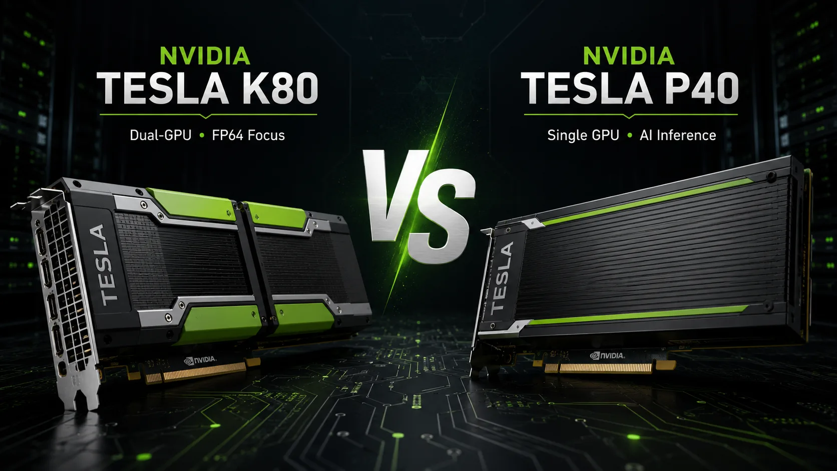
NVIDIA Tesla K80 and Tesla P40 may easily be mistaken for closely related accelerators: both cards are equipped with 24 GB of GDDR5 memory, utilize passive cooling, and are designed for server installations. However, the K80 is a dual-processor model from the Kepler era, primarily designed for scientific calculations, whereas the newer P40 is focused on FP32 and neural network inference. In most modern tasks, the P40 is faster and more convenient; however, the K80 retains one important advantage-FP64 performance.
The Main Difference Lies in Memory
The Tesla K80 combines two GK210 graphics processors. Each GPU has its own 12 GB of memory and operates as a separate CUDA device. The stated specifications of 24 GB cannot be used as a single video buffer: a single task is typically limited to 12 GB unless the program can distribute data across multiple GPUs.
Even with support for two accelerators, some information may be duplicated in the memory of both chips. Therefore, the K80 configuration is not suitable for every computational workload.
The Tesla P40 is simpler: a single GP102 processor has access to all 24 GB. This is more critical than the formal difference in the number of CUDA cores. A larger model or dataset can entirely fit in the memory of a single GPU without manual task partitioning.
| Key Difference | Tesla K80 | Tesla P40 |
|---|---|---|
| Architecture | Kepler | Pascal |
| Configuration | 2 × GK210 | 1 × GP102 |
| Memory | 2 × 12 GB GDDR5 | 24 GB GDDR5 |
| CUDA Cores | 4992 total | 3840 |
| FP32 | up to 8.73 TFLOPS | up to 12 TFLOPS |
| FP64 | up to 2.91 TFLOPS | around 0.37 TFLOPS |
| INT8 | Without specialized mode | up to 47 TOPS |
| Memory Bandwidth | 480 GB/s total | 346 GB/s |
| Power Consumption | 300 W | 250 W |
The total metrics of the K80 also require cautious interpretation. Its 4992 CUDA cores, 480 GB/s bandwidth, and peak teraflops are divided between two GPUs. If an application uses only one GK210, the actual resources are approximately halved.
FP32 and Neural Networks: Clear Victory for P40
In single-precision calculations, the Tesla P40 achieves 12 TFLOPS, while the maximum 8.73 TFLOPS of the K80 are the sum of two processors and depend on the GPU Boost mode.
In practice, the P40's advantage often proves even more pronounced. The program does not need to synchronize two GPUs, exchange data between them, and account for separate memory arrays. If an application does not scale well across multiple accelerators, some resources of the K80 will remain idle.
For inference, the P40 has another strong argument-the INT8 mode with a performance of up to 47 TOPS. NVIDIA positioned this card as a server inference accelerator designed to work with TensorRT. The K80 came before the widespread shift of neural networks to lower-precision calculations and does not offer a comparable INT8 mode.
The P40 lacks Tensor Cores, so it significantly lags behind accelerators of the Volta, Turing, and newer generations in speed for modern models. Nevertheless, within this pair, the P40 is better suited for local inference and other machine learning tasks.
FP64: The Main Advantage of K80
The Tesla K80 was created for high-performance scientific computing, so the GK210 architecture features advanced double-precision blocks. When both processors are loaded, the card can deliver up to 2.91 TFLOPS FP64-almost as much as modern server systems expected from a specialized HPC accelerator.
The GP102 in the P40 was designed with a different priority. Its strength lies in FP32 and integer operations, with FP64 performance being only about one thirty-second of FP32, or approximately 0.37 TFLOPS. Architecturally, GP102 is closer to GP104 than to the compute-oriented GP100 with enhanced double-precision blocks.
Therefore, the K80 may still be more interesting in tasks where FP64 is truly necessary:
- numerical modeling;
- molecular dynamics;
- computational fluid dynamics;
- engineering and scientific CUDA applications;
- legacy projects optimized for multiple Kepler GPUs.
However, this advantage works only in programs capable of loading both processors. A single GK210 has only 12 GB of memory and about half of K80's total computational power.
Drivers and Software Compatibility
The software stack has become one of the main limitations of the K80. NVIDIA has locked the R470 branch as the last one supporting Kepler server accelerators. Newer driver and CUDA versions are no longer intended for this architecture, so often K80 users have to resort to outdated operating systems, libraries, or containers.
The situation is better for the P40. As of 2026, it is still listed among the supported GPUs in modern NVIDIA Data Center driver releases, including R580 and R582 branches. This does not make Pascal a new architecture, but it significantly simplifies the installation of current drivers and the launching of a relatively recent CUDA environment.
With virtualization, the situation is stricter: maintenance for the Tesla P40 within NVIDIA vGPU support has reached its concluding stage, with maintenance support set to end in July 2026. Therefore, purchasing a P40 specifically for a new commercial vGPU server is no longer sensible, even if standard computational drivers continue to support it.
Installation in Workstation
Both cards feature passive heatsinks and rely on a strong directed airflow within the server. In a regular case, a separate fan or duct will be required; natural ventilation is insufficient for accelerators with power consumption of 250-300 W.
Neither the K80 nor P40 has video outputs, meaning a monitor must be connected to integrated graphics or a separate graphics card. It is also essential to verify the type of connector and pinout for power: server Teslas cannot be connected using a standard cable from a gaming graphics card without verification.
The P40 is more practical here not only due to its performance but also because of its lower power consumption-250 W compared to 300 W for the K80.
Conclusion: Tesla K80 or Tesla P40
Tesla P40 is the preferred choice for most tasks. It offers unified 24 GB of memory, higher FP32 speeds, INT8 support, lower power consumption, and significantly more modern software compatibility. The P40 is better suited for inference, CUDA rendering, and applications that require more than 12 GB of memory on a single GPU.
Tesla K80 makes sense only in the narrow niche of FP64. It can significantly outperform the P40 in double-precision scientific calculations but requires software that supports two GPUs, an older branch of drivers, and more complex cooling.
Purchasing a K80 for its nominal 24 GB or large number of CUDA cores is unwise. If the task is not based on FP64 and not optimized for two Kepler processors, the Tesla P40 will be faster, simpler, and more practical.
Advantages
- Higher Boost Clock: 1531MHz (824MHz vs 1531MHz)
- Larger Memory Size: 24GB (12GB vs 24GB)
- Higher Bandwidth: 694.3 GB/s (240.6 GB/s vs 694.3 GB/s)
- More Shading Units: 3840 (2496 vs 3840)
- Newer Launch Date: September 2016 (November 2014 vs September 2016)
Basic
Memory Specifications
Display and Media
Theoretical Performance
Miscellaneous
Benchmarks
Related GPU Comparisons


Share in social media
Or Link To Us
<a href="https://cputronic.com/gpu/compare/nvidia-tesla-k80-vs-nvidia-tesla-p40" target="_blank">NVIDIA Tesla K80 vs NVIDIA Tesla P40</a>