NVIDIA Tesla V100 SXM3 32 GB
Tesla V100 SXM3 32 GB: Faster Than SXM2, but Much More Difficult to Use
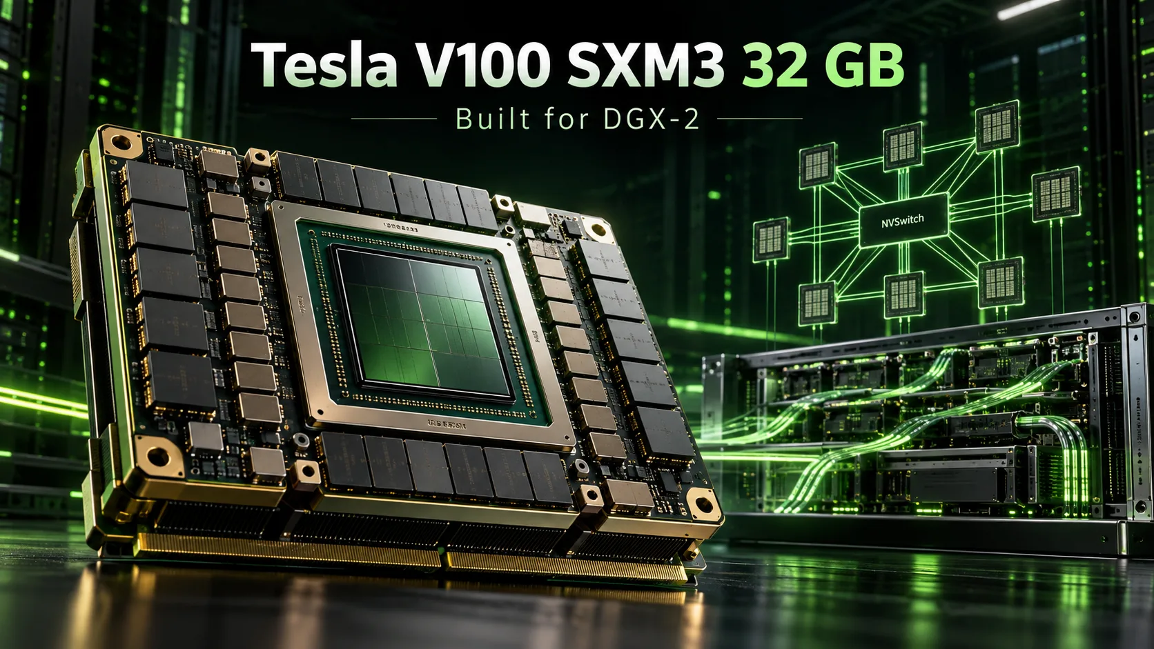
The Tesla V100 SXM3 32 GB is an NVIDIA compute module for the DGX-2 supercomputer and servers based on the HGX-2 platform. NVIDIA introduced the DGX-2 in March 2018. It was built around 16 Volta-based accelerators connected through NVSwitch fabric. Compared with the standard V100 SXM2, the new version featured higher clock speeds, greater memory bandwidth, and a 350 W power limit.
The SXM3 outperforms the SXM2 in specifications, but is considerably less suitable for DIY builds. The module uses a proprietary connector and requires compatible power delivery and cooling, while its operation outside a server platform has barely been tested. Even if it is possible to connect an SXM3 to a conventional computer, its small performance advantage is unlikely to justify the cost.
Position in the Lineup
| Model | Memory | Bandwidth | Boost | Power |
|---|---|---|---|---|
| Tesla V100 PCIe 32 GB | 32 GB HBM2 | 900 GB/s | 1380 MHz | 250 W |
| Tesla V100 SXM2 32 GB | 32 GB HBM2 | 900 GB/s | 1530 MHz | 300 W |
| Tesla V100 SXM3 32 GB | 32 GB HBM2 | 981 GB/s | 1597 MHz | 350 W |
| Tesla V100 SXM3 32 GB H | 32 GB HBM2 | 1134 GB/s | 1702 MHz | 450 W |
All four versions use the same GV100 die with 5120 CUDA cores and 640 tensor cores. The differences lie in clock speeds, power settings, and the connection method.
The standard SXM3 reaches approximately 16.4 TFLOPS in FP32 and 8.2 TFLOPS in FP64. Its memory bandwidth is 9% higher than that of the SXM2, while the GPU clock speed is approximately 4% higher. These differences give the SXM3 an advantage in compute workloads and memory-bandwidth-bound tasks, although the actual gain depends on the workload.
For the DGX-2H, NVIDIA prepared a more powerful SXM3-H variant. Its power limit was increased to 450 W, and its memory bandwidth reaches 1134 GB/s. This is the most powerful V100 version in the SXM form factor.
DGX-2 and NVSwitch
The DGX-2’s main innovation was not the higher GPU clock speed, but the way its GPUs were interconnected.
In the DGX-1, eight SXM2 accelerators were connected directly through NVLink. This topology limited data exchange between individual pairs of GPUs. In the DGX-2, sixteen SXM3 modules were connected to twelve NVSwitches, providing high-speed communication between all accelerators.
The system had 512 GB of total HBM2 memory. Each GPU could access the memory of the others, but this did not turn sixteen accelerators into a single GPU with one shared local buffer. Access latency to remote memory remained higher, and applications required support for distributed computing.
The interconnect bandwidth between the two halves of the system reached 2.4 TB/s. For training large neural networks, this was more important than the small clock-speed increase of individual modules.
The DGX-2 delivered about 2 PFLOPS on its tensor cores, consumed up to 10 kW, and cost $399,000 at launch. NVIDIA continued developing the NVSwitch architecture in subsequent DGX generations, including the DGX A100.
Performance in Modern Workloads
There are virtually no independent tests of the V100 SXM3 in modern language models. Most available results were obtained on the SXM2 and PCIe versions, so the SXM3’s exact advantage in text generation cannot yet be determined.
As a point of reference, a Tesla V100 SXM2 32 GB produces around 32 tokens/s when generating with Qwen3.6-27B in Q4_K_M format using llama.cpp. This is the result for a single GPU, not a system with multiple GPUs.
The SXM3 has 9% greater memory bandwidth, so it could theoretically be faster during generation. However, applying that percentage directly to token generation speed would be incorrect. The result is affected by quantization, context size, software engine, and model characteristics.
The higher clock speeds also provide an advantage in FP32 and FP64 workloads. However, the Volta architecture lags behind newer accelerators in the range of supported compute formats.
The main software limitations are:
- CUDA: The sm_70 compute architecture is supported through CUDA 12.9. Starting with CUDA 13, compiling new GPU kernels for Volta is unavailable.
- Drivers: R580 is NVIDIA’s final driver branch with Volta support.
- BF16: Hardware support is absent, limiting compatibility with modern neural-network training tools.
- FlashAttention 2: The official implementation does not support Volta. Other attention mechanisms must be used instead.
The V100 is still capable of running local LLMs, but launching new models and libraries sometimes requires custom builds.
Can the SXM3 Be Used in a Conventional Computer?
Unlike a PCIe card, an SXM3 module cannot be installed directly into a motherboard slot. It is designed for specialized server boards with the appropriate connector, power-delivery system, and cooling.
SXM3-to-PCIe adapters priced at around $200-300 appear on the secondary market. However, some of them have part numbers associated with the SXM2. There is insufficient independent confirmation that genuine SXM3 modules work reliably with such adapters.
Before buying, verify the following:
- Whether the board supports SXM3 specifically, rather than SXM2.
- Whether the power-delivery system can handle a load of up to 350 W.
- How the module is cooled.
- Whether the GPU is detected by the NVIDIA driver and can sustain a prolonged workload.
A regular photo of the board or a seller’s compatibility claim is not enough. Ideally, obtain nvidia-smi results, a CUDA test, and confirmation that the setup operates reliably specifically with a V100 SXM3.
These problems do not arise when the modules are used as part of a DGX-2 or HGX-2. However, buying an entire server for several outdated accelerators is difficult to justify. The DGX-2 requires a powerful power and cooling infrastructure, and its energy efficiency is inferior to that of modern systems based on the A100 and newer GPUs.
Alternatives
Tesla V100 SXM2 32 GB. The closest alternative with the same memory capacity. Sales on the secondary market have appeared at approximately $450-700, although current listings may be considerably more expensive. SXM2 adapters for PCIe and complete modified cards with cooling are available. The cost of the adapter and the quality of the modification must still be taken into account.
Tesla V100 PCIe 32 GB. A simpler option for a compatible server with PCIe. Based on completed sales, the approximate price range is $650-850, but in autumn 2026 many listings start at $850. The card falls behind the SXM3 in clock speed and memory bandwidth, but does not require specialized SXM boards. It still needs suitable power and forced-air cooling.
Conclusion
The Tesla V100 SXM3 32 GB outperforms the SXM2 in clock speed and memory bandwidth, but its advantages are almost entirely offset by the difficulty of connecting it.
For the owner of a DGX-2 or HGX-2 server, the module remains a useful spare part. For a DIY build, it is of interest only as an experiment requiring verification of adapter, power, and cooling compatibility.
If you need a 32 GB V100 for local neural networks, it is more reasonable to choose an SXM2 with a tested adapter or a ready-made PCIe version. The SXM3 should be purchased only if you have a compatible server platform or a confirmed working connection kit.
GPU Comparison
Compare Tesla V100 SXM3 32 GB with other GPUs
Basic
Memory Specifications
Display and Media
Theoretical Performance
Miscellaneous
Benchmarks
Compared to Other GPU
Share in social media
Or Link To Us
<a href="https://cputronic.com/index.php/gpu/nvidia-tesla-v100-sxm3-32-gb" target="_blank">NVIDIA Tesla V100 SXM3 32 GB</a>