NVIDIA Tesla P100 DGXS
Tesla P100 DGXS: An Accelerator That Exists in Databases but Not on the Market
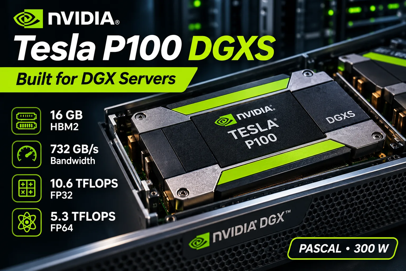
NVIDIA Tesla P100 DGXS appears in graphics card catalogs as a separate model with 16 GB of HBM2, clock speeds of 1328-1480 MHz, and power consumption of 300 W. However, it was not possible to find an official document with these specifications, independent testing, or confirmed sales of this version. At the same time, the P100-DGXS designation appears in NVIDIA drivers, and additional GP100 configurations associated with DGX Station have been found in the company’s diagnostic software.
This makes the P100 DGXS an unusual case: the existence of the corresponding identifier has been confirmed, but the history of the board’s release remains unclear.
How the P100 DGXS Differs from Other Tesla P100 Models
All Tesla P100 models are based on the 16 nm GP100 processor with Pascal architecture and 3584 CUDA cores. Serial versions differ in HBM2 capacity, clock speeds, power consumption, and connection method.
| Model | Memory | Bandwidth | Clocks | Power |
|---|---|---|---|---|
| Tesla P100 PCIe 12 GB | 12 GB | 549 GB/s | 1189-1328 MHz | 250 W |
| Tesla P100 PCIe 16 GB | 16 GB | 732 GB/s | 1189-1328 MHz | 250 W |
| Tesla P100 SXM2 16 GB | 16 GB | 732 GB/s | 1328-1480 MHz | 300 W |
| Tesla P100 DGXS | 16 GB by designation | Not confirmed | 1328-1480 MHz (according to databases) | 300 W (according to databases) |
The DGXS specifications listed in catalogs almost exactly match those of the P100 SXM2. They may have been copied by analogy, but no official NVIDIA specifications for this version could be found.
There is not even confirmation that the DGXS clock speeds actually matched those of the SXM2. Therefore, the figures published in catalogs cannot be used for an accurate performance comparison.
Traces of the P100 DGXS in NVIDIA Documents
The most convincing evidence that this configuration existed is the identifier PCI\VEN_10DE&DEV_15FC. In NVIDIA’s Windows driver database from June 2017, it is listed as Tesla P100-DGXS-16GB.
Additional information can be found in the official NVIDIA DCGM repository, which contains diagnostic settings for server accelerators.
It includes two entries of interest:
- 15FA - DGX Station. A GP100 configuration with a target diagnostic test power of 249 W.
- 15FC - GP100 SKU 201. A separate configuration with a target test power of 299 W.
The second identifier matches the Tesla P100-DGXS-16GB listed in the driver databases. However, the power values in DCGM define the load for diagnostic testing, not the rated TDP.
Thus, NVIDIA did provide for several GP100 configurations, including one designated for DGX Station. However, software entries do not reveal how many physical boards were produced or whether they were delivered to customers.
Connection to NVIDIA DGX Station
The history of the P100 DGXS is complicated by the timeline. NVIDIA introduced the Tesla P100 in April 2016 alongside the DGX-1 server. However, NVIDIA officially announced the DGX Station workstation only on May 10, 2017.
In its initial presentation, the DGX Station was equipped with four Tesla V100 accelerators with 16 GB of HBM2, connected via NVLink. The system used liquid cooling and was priced at $69,000.
At the same time, in October 2017, ServeTheHome reported that the DGX Station used four P100 accelerators during its early stage and later switched to the V100. This conflicts with NVIDIA’s initial official announcement, which already featured Volta accelerators.
The report may have referred to prototypes or preliminary configurations, but no public documents confirming such a shipment could be found.
Therefore, the April 2016 release date for the P100 DGXS found in catalogs cannot be considered confirmed. It refers to the appearance of the GP100, not to a known release of the DGXS model.
Performance: What Can Be Verified
No public test results for the Tesla P100 DGXS itself could be found. Measurements from the production P100 PCIe 16 GB can be used to assess the capabilities of the GP100 architecture.
A comparison published by the llama.cpp community includes results for several specific GPUs when running the Llama 7B Q4_0 model.
| GPU | Prompt processing, tokens/s | Generation, tokens/s |
|---|---|---|
| Tesla V100 32 GB | 2974 | 134.8 |
| GeForce RTX 2080 Ti | 2891 | 107.5 |
| GeForce RTX 3060 12 GB | 2138 | 75.6 |
| GeForce GTX 1080 Ti | 1084 | 62.5 |
| Tesla P100 16 GB | 761 | 58.4 |
Higher is better. The data was published by members of the llama.cpp community. One model was used, but the test systems and program versions differed. The Tesla P100 result is for the PCIe version, not the DGXS.
In this test, the P100 is nearly as fast as the GTX 1080 Ti at generation but falls noticeably behind during prompt processing. One reason is that GP100 lacks DP4A instructions, which accelerate computations with quantized data.
The high bandwidth of HBM2 does not compensate for this limitation. Even at SXM2 clock speeds, the unknown DGXS version would not have gained the missing instructions.
GP100 does have another advantage, however: FP64 performance. The production P100 SXM2 reaches 5.3 TFLOPS of double-precision performance, while the PCIe version reaches 4.7 TFLOPS. This keeps them attractive for some scientific calculations, although the exact performance of the DGXS cannot be established.
Software Support in 2026
All GP100 accelerators have CUDA compute capability 6.0. In modern machine-learning libraries, this is becoming a serious limitation.
The latest version of the CUDA Toolkit that allows applications to be compiled for Pascal is 12.9. Starting with CUDA 13, support for compiling for this architecture has been removed. NVIDIA’s final Pascal driver branch is R580, whose support period ends in 2028.
Older CUDA programs will continue to work with compatible drivers, but new builds of PyTorch and other libraries may not support GP100. The lack of Tensor Cores further limits neural-network performance.
For local language models, 16 GB of HBM2 is still useful, but choosing an accelerator solely based on memory capacity and bandwidth is no longer sufficient.
Can You Buy a P100 DGXS, and What Can Replace It?
No confirmed Tesla P100 DGXS listings could be found on the open secondary market. Its physical design is also unknown: a device identifier alone cannot reveal the connector layout, cooling system, or compatibility with standard motherboards.
If you need an accelerator based on the GP100 architecture, more predictable options are available:
- Tesla P100 PCIe 16 GB. Standard PCIe connectivity, 16 GB of HBM2, and up to 4.7 TFLOPS of FP64 performance. It requires strong directed airflow and suitable power delivery.
- Tesla P100 SXM2 16 GB. Higher performance and NVLink support on compatible servers. A regular computer requires an adapter and separate cooling.
- Tesla V100 SXM2 16 GB. Volta architecture, Tensor Cores, and up to 7.8 TFLOPS of FP64 performance. Considerably more interesting for compatible machine-learning workloads, but it also requires a specialized connection.
For running modern local LLMs, a GeForce RTX with Tensor Cores and a newer architecture is often more practical, even if it has less video memory.
Conclusion
The Tesla P100 DGXS is a real designation in NVIDIA’s software ecosystem, but not a production model confirmed by documentation. The identifiers in the drivers and DCGM indicate the existence of separate GP100 configurations, but their commercial release and technical implementation remain unknown.
Attributing P100 SXM2 specifications to the DGXS without additional evidence would be incorrect. For scientific calculations and CUDA experiments, it is better to choose production P100 PCIe or SXM2 models with known specifications and available test results.
The P100 DGXS is interesting primarily as a little-known part of NVIDIA DGX history, not as a practical purchase option in 2026.
GPU Comparison
Compare Tesla P100 DGXS with other GPUs
Basic
Memory Specifications
Display and Media
Theoretical Performance
Miscellaneous
Benchmarks
Compared to Other GPU
Related GPU Comparisons


Share in social media
Or Link To Us
<a href="https://cputronic.com/index.php/gpu/nvidia-tesla-p100-dgxs" target="_blank">NVIDIA Tesla P100 DGXS</a>