CPU Comparison Result
AMD Ryzen 7 H 255 vs AMD Ryzen 7 8845HS: Almost Identical Chips, But Not the Same Purchase
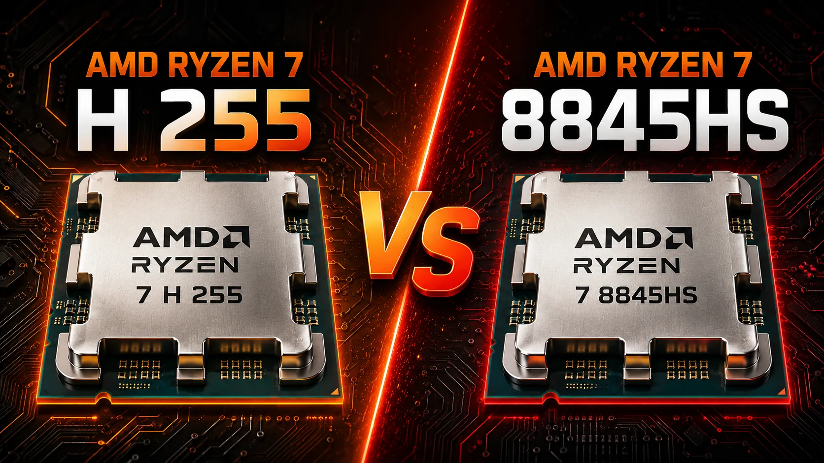
AMD Ryzen 7 H 255 and AMD Ryzen 7 8845HS look like processors from different lines, but inside they are very close. Both belong to the Hawk Point generation, use Zen 4 architecture, have 8 cores, 16 threads, 16 MB of L3 cache, integrated Radeon 780M graphics, and are designed for high-performance laptops or mini-PCs.
However, they are not complete copies. The Ryzen 7 8845HS is a bit faster at maximum frequencies, features a Ryzen AI block, and is more commonly found in global laptop models. The Ryzen 7 H 255 appears to be a closely tuned regional version for the Chinese market: in terms of CPU, it is almost on par, but has lower frequencies and lacks a dedicated AI block.
Main Difference in Two Words
The Ryzen 7 8845HS is a more complete version of Hawk Point. It is better suited if the price is similar, and you want to take full advantage: slightly higher boost frequency, a bit faster Radeon 780M, and support for Ryzen AI.
The Ryzen 7 H 255 offers nearly the same level of CPU performance, but without some extra features. Its value emerges when a specific laptop or mini-PC is significantly cheaper than its counterpart with the Ryzen 7 8845HS.
Brief Comparison
| Characteristic | AMD Ryzen 7 H 255 | AMD Ryzen 7 8845HS |
|---|---|---|
| Architecture | Zen 4 | Zen 4 |
| Family | Hawk Point | Hawk Point |
| Cores / Threads | 8 / 16 | 8 / 16 |
| Base Frequency | 3.8 GHz | 3.8 GHz |
| Boost Frequency | up to 4.9 GHz | up to 5.1 GHz |
| L2 Cache | 8 MB | 8 MB |
| L3 Cache | 16 MB | 16 MB |
| TDP | 45 W | 45 W |
| Configurable TDP | 35-54 W | 35-54 W |
| Process Technology | TSMC 4 nm | TSMC 4 nm |
| Memory | DDR5-5600 / LPDDR5X-7500 | DDR5-5600 / LPDDR5X-7500 |
| Memory Channels | 2 | 2 |
| Integrated Graphics | Radeon 780M | Radeon 780M |
| Graphics Cores | 12 | 12 |
| iGPU Frequency | up to 2600 MHz | up to 2700 MHz |
| Ryzen AI / NPU | No | Yes |
| Positioning | Regional Model | Global Model |
CPU Performance: The Difference Is Smaller Than It Seems
In terms of CPU, the Ryzen 7 H 255 and Ryzen 7 8845HS are very close. They have the same number of cores and threads, the same architecture, the same cache size, and the same power consumption class. The difference in maximum frequency is just 200 MHz in favor of the Ryzen 7 8845HS.
In practice, this does not make the 8845HS a different level of processor. In browsing, office tasks, programming, photo processing, archiving, light editing, and multitasking, both chips will feel very similar. The Ryzen 7 8845HS may be a bit faster in short single-threaded loads, but in longer workloads, much depends not on the processor name but on the cooling and power limits of the specific device.
That is why comparing these processors solely by name is incorrect. A laptop with good cooling on the Ryzen 7 H 255 may prove to be more stable under prolonged load than a thin model on Ryzen 7 8845HS with strict temperature limits.
Integrated Graphics: Radeon 780M in Both Cases
Both processors feature the Radeon 780M – one of AMD's most successful integrated graphics solutions for laptops and mini-PCs. This is an important advantage, as such an iGPU is suitable not only for desktop tasks and video but also for light gaming.
You can play esports titles, older AAA games, and certain modern games at low to medium settings on the Radeon 780M. Of course, this is not a replacement for a discrete graphics card, but for a compact computer without a separate GPU, the performance level is quite commendable.
The integrated graphics on the Ryzen 7 8845HS runs at up to 2700 MHz, while the Ryzen 7 H 255 runs at up to 2600 MHz. There is a difference, but it's small. In real gaming scenarios, memory will be more important: dual-channel mode, DDR5 or LPDDR5X speeds, power limits, and cooling quality can affect FPS more strongly than a 100 MHz difference in GPU core frequency.
If the price is the same, it makes more sense to choose the Ryzen 7 8845HS for gaming on integrated graphics. If the device on the Ryzen 7 H 255 is significantly cheaper, the overpayment just for a slightly faster iGPU is not always justified.
Ryzen AI: The Main Advantage of Ryzen 7 8845HS
The most important distinction between these processors is the presence of Ryzen AI in the Ryzen 7 8845HS. This is a separate NPU block that can accelerate local AI tasks: image processing, noise reduction, background effects, certain Windows features, and applications that leverage neural computation.
The Ryzen 7 H 255 lacks such a block. For everyday tasks, this is not critical: browsing, gaming, office work, coding, multimedia, and most regular tasks function smoothly without an NPU. However, if a laptop is purchased for several years, having Ryzen AI in the 8845HS looks more promising.
It is essential not to overestimate this point. Ryzen AI does not make the 8845HS drastically faster in games or standard programs. But it is an additional capability that the H 255 simply lacks. Therefore, at equal prices, the 8845HS appears to be the more sensible purchase.
Why H 255 Is So Similar to 8845HS
The Ryzen 7 H 255 does not appear as a new generation but rather as a closely tuned version of the already familiar Hawk Point platform for specific OEM devices and the regional market. Thus, it does not feel like a standalone step between generations but rather occupies the niche of a more accessible alternative to the 8845HS without Ryzen AI.
That is why the H 255 should not be considered a weak or unusual processor. It is a standard 8-core Zen 4 with powerful integrated graphics. It simply seems more stripped down in additional capabilities than the Ryzen 7 8845HS.
What’s More Important When Buying a Device
When choosing between the Ryzen 7 H 255 and Ryzen 7 8845HS, one cannot look only at the processor. For laptops and mini-PCs, other parameters are very important:
- Cooling system;
- Power limits of the processor;
- Type and speed of the RAM;
- Operation of memory in dual-channel mode;
- Screen quality;
- Port selection;
- Noise level;
- Price of the specific model.
If you have two almost identical devices, the Ryzen 7 8845HS is better. However, if the model with the Ryzen 7 H 255 is cheaper, has good cooling, fast memory, and a decent chassis, it may be the more cost-effective purchase.
What to Choose
| Scenario | Best Choice |
|---|---|
| Price almost the same | Ryzen 7 8845HS |
| Need for Ryzen AI/NPU | Ryzen 7 8845HS |
| Buying a laptop for several years | Ryzen 7 8845HS |
| Gaming on integrated graphics | Ryzen 7 8845HS, but difference small |
| Maximum price effectiveness | Ryzen 7 H 255 |
| Mini-PC without discrete graphics | Both are suitable |
| Office, browsing, coding, multimedia | Both are suitable |
| If H 255 is significantly cheaper | Ryzen 7 H 255 |
Conclusion
The AMD Ryzen 7 8845HS is the default choice. It is slightly faster at frequencies, features a faster version of the Radeon 780M, supports Ryzen AI, and appears to be a more versatile option for laptops or mini-PCs.
The AMD Ryzen 7 H 255 is the price choice. In terms of CPU performance, it is very close to the 8845HS, uses the same Zen 4 architecture, and the same strong integrated graphics Radeon 780M. Its main drawbacks are the lack of Ryzen AI and somewhat lower frequencies.
If the devices are priced similarly, it’s better to choose the Ryzen 7 8845HS. If the Ryzen 7 H 255 is significantly cheaper, and the laptop or mini-PC has good cooling and fast memory, it may be the more sensible purchase.
Advantages
- Newer Launch Date: January 2025 (January 2025 vs December 2023)
Basic
CPU Specifications
Memory Specifications
GPU Specifications
Miscellaneous
Benchmarks
Related CPU Comparisons
Share in social media
Or Link To Us
<a href="https://cputronic.com/cpu/compare/amd-ryzen-7-h-255-vs-amd-ryzen-7-8845hs" target="_blank">AMD Ryzen 7 H 255 vs AMD Ryzen 7 8845HS</a>


