Intel Core Ultra 7 270K Plus
vs
Intel Core Ultra 9 285K


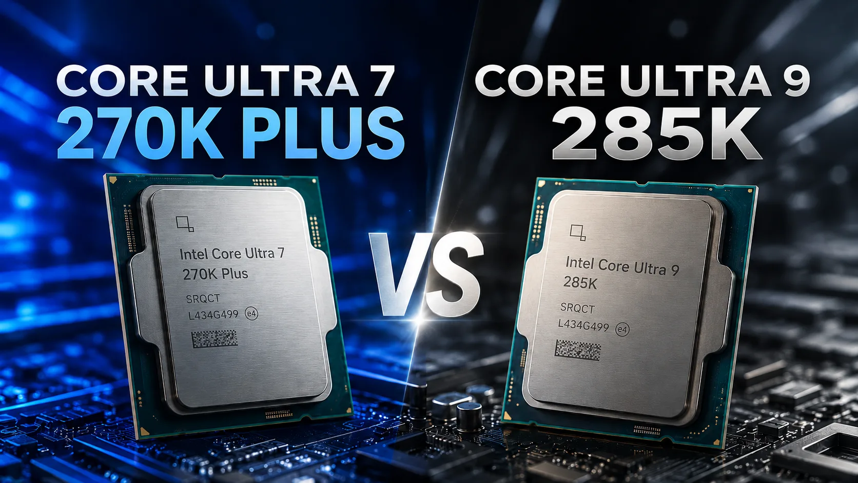
CPU Comparison Result
Intel Core Ultra 7 270K Plus vs Core Ultra 9 285K: Almost a flagship for less money
The Intel Core Ultra 9 285K formally remains the flagship of the Arrow Lake desktop lineup, but the Core Ultra 7 270K Plus makes the choice less obvious. It has the same 8P + 16E configuration, similar clock speeds, faster official memory support, and a significantly lower recommended price.
The main question is simple: does the Core Ultra 9 285K have enough advantages to justify the serious markup?
Key Differences
Both processors are built on the Arrow Lake architecture and use the LGA1851 platform. They have the same core configuration: 24 cores, 24 threads, 8 performance P-cores, and 16 energy-efficient E-cores. The cache size, base power, maximum turbo power, and socket are also the same.
Therefore, the table below lists only the real differences.
| Parameter | Intel Core Ultra 7 270K Plus | Intel Core Ultra 9 285K |
|---|---|---|
| Max Turbo | up to 5.5 GHz | up to 5.7 GHz |
| P-core Max Turbo | up to 5.4 GHz | up to 5.5 GHz |
| E-core Max Turbo | up to 4.7 GHz | up to 4.6 GHz |
| Official Memory Support | DDR5-7200 | DDR5-6400 |
| Recommended Price | $289-299 | $589-599 |
| Launch Date | Q1 2026 | Q4 2024 |
On paper, the Core Ultra 9 285K is faster due to its higher peak frequency, but the difference is less significant than it seems from the name. For P-core Max Turbo, the advantage is only 100 MHz. However, the Core Ultra 7 270K Plus has a higher E-core frequency, faster official memory, and a much lower price.
Essentially, Intel has created a situation where the Ultra 7 starts to look more rational than the Ultra 9. The Core Ultra 7 270K Plus is seen not just as an ordinary lower model but as an almost flagship version at a lower price.
Performance
In multi-threaded tasks, both processors are very close. This makes sense: they have the same 8P + 16E configuration, the same number of threads, and the same cache size. Rendering, video encoding, compilation, and heavy multitasking are well suited to both CPUs.
The Core Ultra 7 270K Plus can match or slightly outperform the Core Ultra 9 285K in certain tests. But this isn't a story of a large gap. It's more realistic to talk about a few percent difference, depending on the test, BIOS, memory, and motherboard settings.
In single-threaded workloads, the Core Ultra 9 285K may still be slightly ahead due to its higher peak frequency. However, in everyday usage, this advantage is hardly noticeable.
| Scenario | What Happens in Practice |
|---|---|
| Multi-threaded Work | 270K Plus is often close to 285K, sometimes slightly ahead |
| Single-thread | 285K can be slightly faster due to frequency |
| Power Consumption | 270K Plus is not necessarily more efficient |
| Price/Performance | 270K Plus is significantly better value |
Gaming
In gaming, both processors are limited not so much by each other but by the graphics card, memory, and platform features. With a powerful graphics card and good DDR5, they are suitable for modern games, streaming, and background tasks, but the advantage of Core Ultra 9 285K over 270K Plus is usually too small to justify the significant surcharge.
Arrow Lake has had a complicated history with gaming performance. At launch, the platform received criticism for latency and not always expected performance in games. BIOS updates, memory tweaks, and optimizations have partially improved the situation, but Ryzen X3D processors can still outperform it in maximum FPS scenarios.
If a versatile processor for gaming and work is needed, the Core Ultra 7 270K Plus looks like a solid choice. If maximum frames are the priority at any cost, it’s worth comparing not just these two Intel models but also alternatives with 3D V-Cache.
Platform, Power, and Cooling
From a platform perspective, there’s almost no difference. Both processors use LGA1851, are designed for Intel 800-series motherboards, have integrated Intel Graphics with 4 Xe-cores, and an Intel AI Boost NPU with 13 TOPS. The integrated graphics are suitable for display output, diagnostics, and hardware video blocks, but cannot replace a discrete GPU.
Thunderbolt, Wi-Fi 7, USB options, networking, and additional interfaces should be checked based on the specific motherboard. Here, not only the processor but also the controllers, layout, and quality of the board matter.
In terms of power, both CPUs are similar: 125W base power and up to 250W Maximum Turbo Power. The Core Ultra 7 270K Plus should not be automatically considered cooler: under heavy load, it can consume at levels similar to or even higher than the 285K. Both require a good cooler or liquid cooling solution.
What to Choose in the End
The Core Ultra 7 270K Plus appears to be the most sensible choice for a new LGA1851 build. It offers nearly the same level of performance as the Core Ultra 9 285K but at a significantly lower recommended price.
It should be considered for a versatile PC: gaming, editing, streaming, compilation, heavy multitasking. Saving on the processor is often more advantageous here, allowing investment in a graphics card, memory, SSD, or higher-quality motherboard.
The Core Ultra 9 285K remains a fast processor, but its advantage is too thin. It makes sense only at a significant discount, a small surcharge in a pre-built system, or if the higher Intel model is specifically required.
The conclusion is simple: for most new builds, the Intel Core Ultra 7 270K Plus appears to be the more rational choice. The Core Ultra 9 285K should only be considered at a good price or if the surcharge is not an issue.
Advantages
- Newer Launch Date: March 2026 (March 2026 vs December 2024)
- Higher Performance-core Max Turbo Frequency: 5.7 GHz (5.5 GHz vs 5.7 GHz)
Basic
CPU Specifications
Memory Specifications
GPU Specifications
Interfaces and Ports
Benchmarks
Related CPU Comparisons


Share in social media
Or Link To Us
<a href="https://cputronic.com/cpu/compare/intel-core-ultra-7-270k-plus-vs-intel-core-ultra-9-285k" target="_blank">Intel Core Ultra 7 270K Plus vs Intel Core Ultra 9 285K</a>