AMD Ryzen AI 9 365
vs
AMD Ryzen 7 H 255
CPU Comparison Result
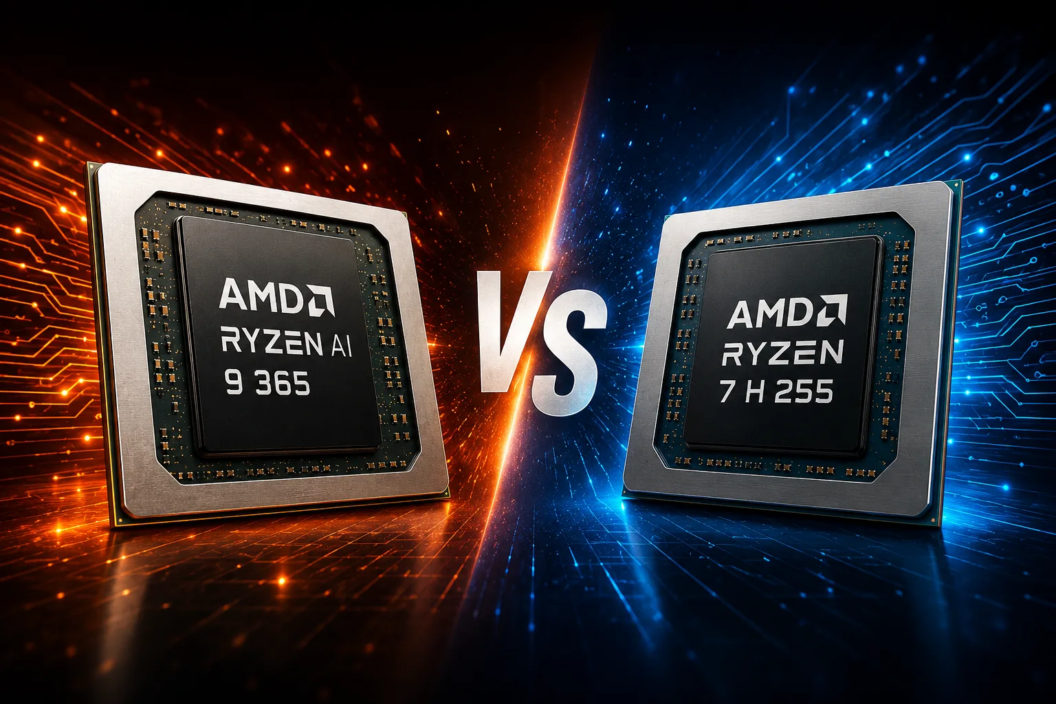
AMD Ryzen AI 9 365 vs Ryzen 7 H 255: Zen 5 is Faster, But Power Matters
The Ryzen AI 9 365 is newer, faster per core, and equipped with more powerful graphics featuring a dedicated NPU. However, the Ryzen 7 H 255 is more commonly found in mini PCs with a high power limit, which allows the older Zen 4 to sometimes outperform it in prolonged multi-threaded tests.
The outcome depends not only on the processor but also on the specific device; systems with the Ryzen AI 9 365 can vary in performance by nearly 1.5 times due to power and cooling settings.
Key Differences
| Parameter | AMD Ryzen AI 9 365 | AMD Ryzen 7 H 255 |
|---|---|---|
| Architecture | Zen 5 + Zen 5c | Zen 4 |
| Cores / Threads | 10 / 20 | 8 / 16 |
| Core Configuration | 4 Zen 5 + 6 Zen 5c | 8 Zen 4 |
| Max Clock Speed | Up to 5.0 GHz | Up to 4.9 GHz |
| L2 Cache | 10 MB | 8 MB |
| L3 Cache | 24 MB | 16 MB |
| Nominal TDP | 28 W, configurable by manufacturers | 45 W, limits in mini-PCs may be higher |
| Integrated Graphics | Radeon 880M | Radeon 780M |
| GPU Architecture | RDNA 3.5 | RDNA 3 |
| GPU Compute Units | 12 | 12 |
| Max GPU Clock Speed | Up to 2.9 GHz | Up to 2.6 GHz |
| NPU | XDNA 2, up to 50 TOPS | No |
| Typical Devices | Laptops | Mini PCs and larger mobile systems |
The Ryzen AI 9 365 features two additional cores and four more threads, increased cache, newer graphics, and a separate neural processor. The Ryzen 7 H 255 is technically simpler but can sustain high power usage for longer periods in mini PCs.
Performance in Specific Devices
The results show the performance of complete systems and are influenced by cooling, memory, firmware, and power settings.
| Device | Processor | Geekbench 6 Single | Geekbench 6 Multi | Cinebench R23 Multi |
|---|---|---|---|---|
| Asus Zenbook S 16 | Ryzen AI 9 365 | 2778 | 12 627 | 11 462 |
| Lenovo Yoga Pro 7 14 G9 | Ryzen AI 9 365 | 2815 | 14 118 | 18 748 |
| MSI Prestige A16 AI+ | Ryzen AI 9 365 | 2830 | 14 189 | 18 069 |
| Beelink SER9 Pro | Ryzen 7 H 255 | 2546 | 12 825 | 16 402 |
| GMKtec K12, 65 W profile | Ryzen 7 H 255 | 2440 | 12 226 | 16 001 |
Single-Thread Performance
The Ryzen AI 9 365 is consistently faster per core. Laptops with it score between 2778-2830 points in Geekbench 6 Single, while systems with the Ryzen 7 H 255 score between 2440-2546 points.
The advantage of Zen 5 is approximately 9-16% depending on the devices. This is noticeable in everyday applications, older games, emulators, and programs with poor parallelization.
In typical use, the difference is minor, but the winner remains constant: the Ryzen AI 9 365 is faster in all examined systems.
Multi-Thread Performance
In prolonged workloads, the results depend much more on the chassis and power limit.
The Ryzen AI 9 365 in the thin Asus Zenbook S 16 scores only 11,462 points in Cinebench R23 Multi. The Beelink SER9 Pro mini PC with the Ryzen 7 H 255 scored 16,402 points, while the GMKtec K12 scored around 16,001 points.
In this comparison, mini PCs with the Ryzen 7 H 255 are almost 40% faster than the Zenbook S 16.
However, more powerful laptops with the Ryzen AI 9 365 change the narrative. The Lenovo Yoga Pro 7 scores 18,748 points, while the MSI Prestige A16 AI+ scores 18,069 points. This is about 10-17% higher than the results from systems with the Ryzen 7 H 255.
Within one Lenovo Yoga Pro 7, the score of the Ryzen AI 9 365 varies approximately from 13,698 points at a 25 W profile to 18,748 points at 54 W and 19,091 points in maximum mode. The processor itself remains the same - only the available power and cooling change.
Therefore, it is more accurate to discuss not an unconditional advantage of one chip but three scenarios:
- With comparable sustained power, the Ryzen AI 9 365 is usually faster;
- In a thin laptop, it may fall behind the Ryzen 7 H 255 in a mini PC;
- Cooling systems influence multi-thread performance more than generational differences themselves.
Integrated Graphics
Both processors are equipped with graphics featuring 12 compute units. The Radeon 880M uses RDNA 3.5 architecture and operates at a frequency of up to 2.9 GHz, while the Radeon 780M is based on RDNA 3 and boosts up to 2.6 GHz.
| Device | Graphics | 3DMark Time Spy Graphics |
|---|---|---|
| Lenovo Yoga Pro 7 14 G9 | Radeon 880M | 3423 |
| MSI Prestige A16 AI+ | Radeon 880M | 3464 |
| Beelink SER9 Pro | Radeon 780M | 3077 |
In the reviewed devices, the Radeon 880M is approximately 11-13% faster. The difference is noticeable, but both graphics systems remain in the same class.
They are suitable for esports games, older titles, and modern games at low settings. The overall performance also depends on the speed of RAM and power limits.
The Radeon 880M is the better option, but it does not elevate the system to a different class of gaming performance.
NPU
The Ryzen AI 9 365 features an XDNA 2 neural processor with a performance of up to 50 TOPS. The Ryzen 7 H 255 does not have a dedicated NPU.
This is important for compatible local AI functions: noise cancellation, image processing, speech recognition, and Windows tools. However, the NPU does not accelerate regular rendering, gaming, and applications that do not utilize it.
For a traditional mini PC, the lack of an NPU may not be significant. For a new laptop designed for local AI functions, the Ryzen AI 9 365 is considerably more forward-looking.
Devices and Pricing
The Ryzen AI 9 365 is primarily found in laptops:
- Asus Zenbook S 16;
- Lenovo Yoga Pro 7 14;
- MSI Prestige A16 AI+.
The price for such models usually starts around $1500-1600, although it varies significantly depending on the screen, memory size, and configuration.
The Ryzen 7 H 255 is more frequently installed in mini PCs:
- Beelink SER9 Pro;
- GMKtec K12;
- Minisforum AI X1.
The GMKtec K12 was offered starting at approximately $409 in the barebone version and around $549 with 32 GB of memory and a 1 TB SSD. The Beelink SER9 Pro was seen for about $510-520.
Directly comparing the prices of laptops and mini PCs is not fair. A laptop already includes a screen, battery, and keyboard, while a mini PC typically offers more ports, replaceable memory, and multiple storage options.
Who Should Choose Systems with These Processors
Choose Ryzen AI 9 365 if:
- You need a laptop;
- High single-core performance is important;
- You require faster integrated graphics;
- You need an NPU with 50 TOPS;
- Mobility and battery operation are priorities.
Choose Ryzen 7 H 255 if:
- You need a compact desktop;
- The mini PC is significantly cheaper;
- The ability to replace memory and storage is important;
- High performance under prolonged load is required;
- An NPU is not necessary.
Conclusion
The AMD Ryzen AI 9 365 is about 9-16% faster per core, and its Radeon 880M outperforms the Radeon 780M by approximately 11-13%. Moreover, the new processor has two additional cores, increased cache, and a 50 TOPS NPU.
In multi-threaded tasks, there isn't a universal winner. Powerful laptops with the Ryzen AI 9 365 outperform systems with the Ryzen 7 H 255 by about 10-17%, but the thin Asus Zenbook S 16 significantly lags behind.
The Ryzen AI 9 365 is better suited for modern laptops. The Ryzen 7 H 255 remains a sensible choice for budget mini PCs, especially if upgradeability and sustained high performance are important.
Advantages
- More Total Cores: 10 (10 vs 8)
- Larger L3 Cache: 24 MB (24 MB vs 16 MB shared)
- Newer Launch Date: July 2025 (July 2025 vs January 2025)
Basic
CPU Specifications
Memory Specifications
GPU Specifications
Interfaces and Ports
Miscellaneous
Benchmarks
Related CPU Comparisons


Share in social media
Or Link To Us
<a href="https://cputronic.com/cpu/compare/amd-ryzen-ai-9-365-vs-amd-ryzen-7-h-255" target="_blank">AMD Ryzen AI 9 365 vs AMD Ryzen 7 H 255</a>